IIC协议举例
- 常用IIC协议使用地方
- 常见IIC协议的注意点
- 24LC64芯片读写命令的时序图
- eeprom控制器的系统框图
- 时序图设计
- 代码设计
- EEPROM控制器测试模块的代码
- 结束语
常用IIC协议使用地方
熟悉一个协议一定要知道这个协议应该用到什么地方,IIC协议作为飞利浦公司定义的一个慢速传输协议,常用于:
1、芯片寄存器的配置;
2、eeprom的读写;
本次实验我们将使用eeprom来讲解IIC协议以及FPGA代码的编写,本次实验所用到的软硬件环境如下:
硬件:黑金A7102开发板
软件:vivado 19.1
黑金A7102开发板上eeprom的型号位:24LC04,是单字节地址的eeprom。再比如小梅哥AC620开发板上的eeprom为双字节地址的器件。为了让同学们了解两者,本次实验我们以24LC64为例进行实验,然后更改为单字节的24LC04并在板上验证。
常见IIC协议的注意点
1、总线空闲状态:SDA为高电平,SCL为高电平
2、起始位:SCL为高电平时,SDA产生一个下降沿
3、结束位:SCL为高电平时,SDA产生一个上升沿
IIC总线的三种模式如下:
标准模式:100Kbit/s
快速模式:400Kbit/s
高速模式:3.4Mbit/s
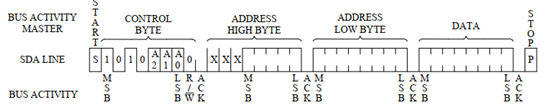
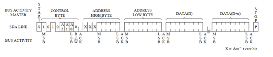
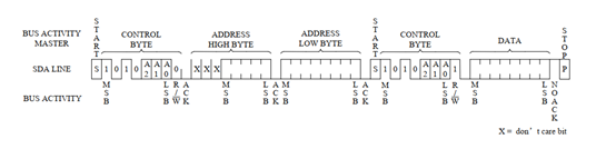
24LC64芯片读写命令的时序图
24LC64芯片的单字节写命令时序图如下:
连续字节写命令如下:
24LC64芯片的单字节读命令时序图如下:
连续字节读命令如下:
同理这里也给出24LC04命令的读写时序图,单字节写命令时序图如下:
连续字节写命令如下:
24LC04芯片的单字节读命令时序图如下:
连续字节读命令如下:

eeprom控制器的系统框图
该eeprom控制器的系统框图主要由以下四部分构成:
顶层模块:
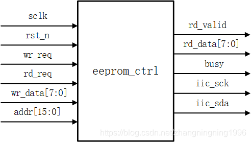
详细大家从引脚的定义便可以明白该信号的作用,如果实在明白不了可以进群拿到现成的工程代码,进行仿真观察。
sclk:主时钟信号——50Mhz
rst_n:复位信号低电平有效
wr_reg:写请求信号,单时钟脉冲
rd_req:读请求信号,单时钟脉冲
wr_data:写数据
addr:读写eeprom地址
rd_valid:读数据有效信号,单时钟脉冲
rd_data:读出来的eeprom数据
busy:控制器内部忙信号,1为忙
iic_sck:IIC协议时钟线
iic_sda:IIC协议的数据线
该模块作为顶层模块,主要包括以下三种模块:
1、eeprom_read模块:eeprom的读模块
2、eeprom_write模块:eeprom的写模块
3、ctrl模块:eeprom的读写判决模块
eeprom_read模块的系统框图如下:
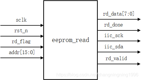
信号的含义如下:
rd_flag:读触发信号,高电平有效
rd_done:读操作结束信号
eeprom_write模块的系统框图如下:
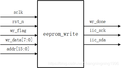
信号的含义如下:
wr_flag:写触发信号,高电平有效
wr_done:写操作完成信号
ctrl模块的系统框图如下:
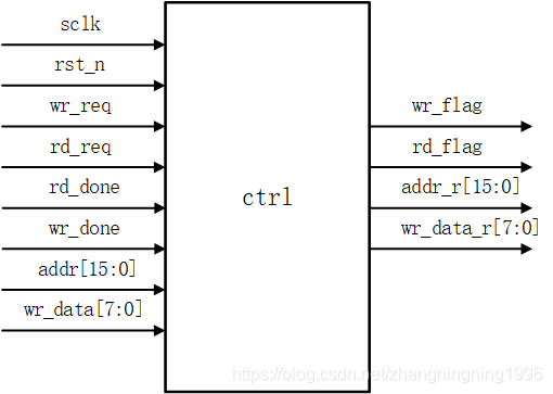
信号的含义如下::
wr_data_r:数据寄存信号
addr_r:地址寄存信号
时序图设计
eeprom_write模块的时序图设计如下:
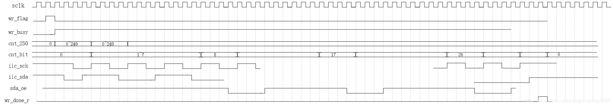
该时序图知识近似设计,结合该时序图于代码可以直接理解该模块的编写。
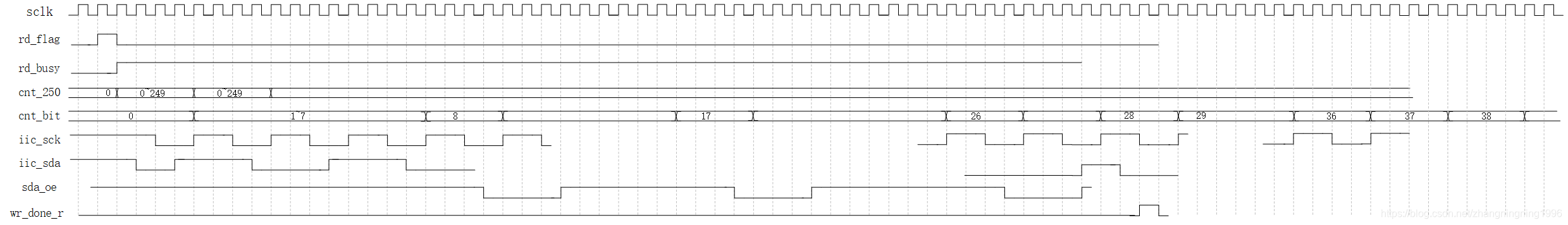
eeprom_read模块的时序图设计如下:
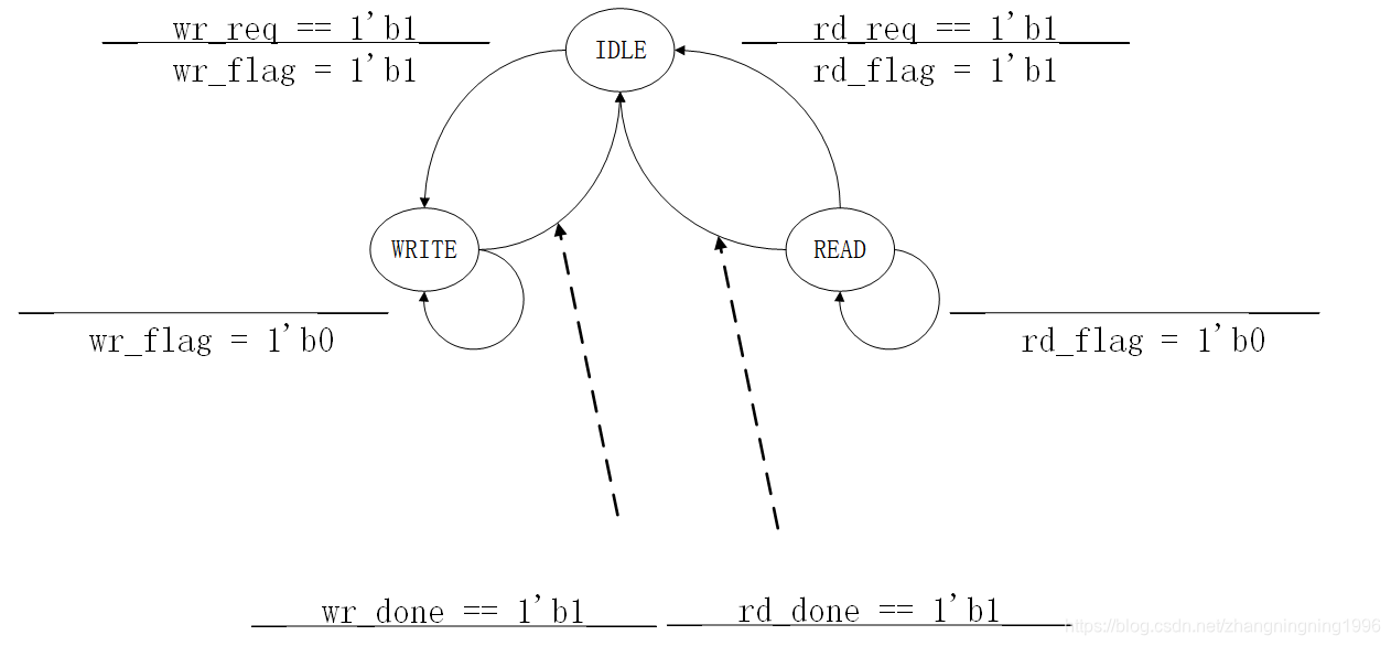
ctrl模块的状态机为:
代码设计
这里将给出整个控制器的逻辑代码,如下:
top模块的代码如下:
`timescale 1ns / 1ps
// *********************************************************************************
// Project Name : OSXXXX
// Author       : zhangningning
// Email        : nnzhang1996@foxmail.com
// Website      :
// Module Name  : top.v
// Create Time  : 2020-01-14 11:23:02
// Editor       : sublime text3, tab size (4)
// CopyRight(c) : All Rights Reserved
//
// *********************************************************************************
// Modification History:
// Date             By              Version                 Change Description
// -----------------------------------------------------------------------
// XXXX       zhangningning          1.0                        Original
//
// *********************************************************************************module top(input                   sclk            ,input                   rst_n           ,input                   wr_req          ,input                   rd_req          ,input           [15:0]  addr            ,output  wire    [ 7:0]  rd_data         ,output  wire            rd_valid        ,input           [ 7:0]  wr_data         ,output  wire            busy            ,output  wire            iic_sck         ,inout                   iic_sda
);//========================================================================================\
//**************Define Parameter and  Internal Signals**********************************
//========================================================================================/
wire                       rd_done         ;
wire                       wr_done         ;
wire			           wr_flag         ;
wire			           rd_flag         ;
wire			   [15:0]  addr_r          ;
wire			   [ 7:0]  wr_data_r       ;
wire     				   iic_sck_wr 	   ;
wire     				   iic_sck_rd 	   ;//========================================================================================\
//**************     Main      Code        **********************************
//========================================================================================/
ctrl ctrl_inst(.sclk                   (sclk                   ),.rst_n                  (rst_n                  ),.wr_req                 (wr_req                 ),.rd_req                 (rd_req                 ),.rd_done                (rd_done                ),.wr_done                (wr_done                ),.addr                   (addr                   ),.iic_sck_wr 			(iic_sck_wr 			),.iic_sck_rd 			(iic_sck_rd 			),.wr_data                (wr_data                ),.wr_flag         		(wr_flag         		),.rd_flag         		(rd_flag         		),.addr_r          		(addr_r          		),.wr_data_r       		(wr_data_r       		),.busy                   (busy                   ),.iic_sck				(iic_sck				)
);eeprom_write eeprom_write_inst(.sclk            		(sclk            		),.rst_n           		(rst_n           		),.wr_flag         		(wr_flag				),.wr_data         		(wr_data_r				),.addr            		(addr_r					),.wr_done         		(wr_done 				),.iic_sck         		(iic_sck_wr 			),.iic_sda     			(iic_sda				)
);eeprom_read eeprom_read_inst(.sclk            		(sclk            		),.rst_n           		(rst_n           		),.rd_flag         		(rd_flag         		),.rd_data         		(rd_data         		),.rd_valid 		 		(rd_valid 		 		),.addr            		(addr_r 				),.rd_done         		(rd_done         		),.iic_sck         		(iic_sck_rd       		),.iic_sda     			(iic_sda     			)
);endmodule
eeprom_write模块的代码如下:
`timescale 1ns / 1ps
// *********************************************************************************
// Project Name : OSXXXX
// Author       : zhangningning
// Email        : nnzhang1996@foxmail.com
// Website      :
// Module Name  : eeprom_write.v
// Create Time  : 2020-01-14 09:51:46
// Editor       : sublime text3, tab size (4)
// CopyRight(c) : All Rights Reserved
//
// *********************************************************************************
// Modification History:
// Date             By              Version                 Change Description
// -----------------------------------------------------------------------
// XXXX       zhangningning          1.0                        Original
//
// *********************************************************************************module eeprom_write(input                   sclk            ,input                   rst_n           ,input                   wr_flag         ,input           [ 7:0]  wr_data         ,input           [15:0]  addr            ,output  reg             wr_done         ,output  reg             iic_sck         ,inout                   iic_sda
);//========================================================================================\
//**************Define Parameter and  Internal Signals**********************************
//========================================================================================/
parameter  DIV_CNT      =   249             ;
parameter  DEVICE_ADDR  =   8'hA0           ;reg                         wr_busy         ;
reg                 [ 7:0]  cnt_250         ;
reg                 [ 5:0]  cnt_bit         ;
reg                         sda_oe          ;
reg                         iic_sda_r       ;//========================================================================================\
//**************     Main      Code        **********************************
//========================================================================================/
assign  iic_sda         =       (sda_oe && !iic_sda_r) ? 1'b0:1'bz;always @(posedge sclk or negedge rst_n)if(rst_n == 1'b0)wr_busy         <=      1'b0;else if(wr_flag == 1'b1)wr_busy         <=      1'b1;else if(wr_done == 1'b1)wr_busy         <=      1'b0;always @(posedge sclk)if(rst_n == 1'b0)cnt_250         <=      8'd0;     else if(cnt_250 == DIV_CNT || wr_done == 1'b1)cnt_250         <=      8'd0;else if(wr_busy == 1'b1)cnt_250         <=      cnt_250 + 1'b1;elsecnt_250         <=      cnt_250;always @(posedge sclk or negedge rst_n)if(rst_n == 1'b0)cnt_bit         <=      5'd0;else if(wr_done == 1'b1)cnt_bit         <=      5'd0;else if(cnt_250 == DIV_CNT)cnt_bit         <=      cnt_bit + 1'b1;else cnt_bit         <=      cnt_bit;always @(posedge sclk or negedge rst_n)if(rst_n == 1'b0)iic_sck         <=      1'b1;else if(cnt_bit != 'd37 && cnt_250 == DIV_CNT/2)iic_sck         <=      1'b0;else if(cnt_250 == 'd0)iic_sck         <=      1'b1;elseiic_sck         <=      iic_sck;always @(posedge sclk or negedge rst_n)if(rst_n == 1'b0)sda_oe          <=      1'b1;else if((cnt_bit == 8 || cnt_bit == 17 || cnt_bit == 26 || cnt_bit == 35) && cnt_250 == (DIV_CNT/2 + DIV_CNT/4))sda_oe          <=      1'b0;else if((cnt_bit == 9 || cnt_bit == 18 || cnt_bit == 27|| cnt_bit == 36) && cnt_250 == (DIV_CNT/2 + DIV_CNT/4))sda_oe          <=      1'b1;elsesda_oe          <=      sda_oe;always @(posedge sclk or negedge rst_n)if(rst_n == 1'b0)iic_sda_r       <=      1'b1;else case(cnt_bit)0   :               if(cnt_250 == (DIV_CNT/4))iic_sda_r       <=      1'b0;else if(cnt_250 == (DIV_CNT/2 + DIV_CNT/4))iic_sda_r       <=      DEVICE_ADDR[7-cnt_bit];elseiic_sda_r       <=      iic_sda_r;                                  1,2,3,4,5,6     :   if(cnt_250 == (DIV_CNT/2 + DIV_CNT/4))iic_sda_r       <=      DEVICE_ADDR[7-cnt_bit];elseiic_sda_r       <=      iic_sda_r;7               :   if(cnt_250 == (DIV_CNT/2 + DIV_CNT/4))iic_sda_r       <=      1'b0;elseiic_sda_r       <=      iic_sda_r;8               :   if(cnt_250 == (DIV_CNT/2 + DIV_CNT/4))iic_sda_r       <=      1'b0;else iic_sda_r       <=      iic_sda_r;12,13,14,15,16  :   if(cnt_250 == (DIV_CNT/2 + DIV_CNT/4))iic_sda_r       <=      addr[24-cnt_bit];elseiic_sda_r       <=      iic_sda_r;17              :   if(cnt_250 == (DIV_CNT/2 + DIV_CNT/4))iic_sda_r       <=      1'b0;else iic_sda_r       <=      iic_sda_r;18,19,20,21,22,23,24,25 :if(cnt_250 == (DIV_CNT/2 + DIV_CNT/4))iic_sda_r       <=      addr[25-cnt_bit];elseiic_sda_r       <=      iic_sda_r;26              :   if(cnt_250 == (DIV_CNT/2 + DIV_CNT/4))iic_sda_r       <=      1'b0;else iic_sda_r       <=      iic_sda_r;27,28,29,30,31,32,33,34 :if(cnt_250 == (DIV_CNT/2 + DIV_CNT/4))iic_sda_r       <=      wr_data[34-cnt_bit];elseiic_sda_r       <=      iic_sda_r;35              :   if(cnt_250 == (DIV_CNT/2 + DIV_CNT/4))iic_sda_r       <=      1'b0;else iic_sda_r       <=      iic_sda_r;36              :   iic_sda_r       <=      iic_sda_r;37              :   if(cnt_250 == (DIV_CNT/4))iic_sda_r       <=      1'b1;default         :   iic_sda_r       <=      1'b1;endcase always @(posedge sclk or negedge rst_n)if(rst_n == 1'b0)wr_done         <=      1'b0;else if(cnt_bit == 'd37 && cnt_250 == (DIV_CNT/2)) wr_done         <=      1'b1;elsewr_done         <=      1'b0;endmodule
eeprom_read模块的代码如下:
`timescale 1ns / 1ps
// *********************************************************************************
// Project Name : OSXXXX
// Author       : zhangningning
// Email        : nnzhang1996@foxmail.com
// Website      :
// Module Name  : eeprom_read.v
// Create Time  : 2020-01-14 09:52:00
// Editor       : sublime text3, tab size (4)
// CopyRight(c) : All Rights Reserved
//
// *********************************************************************************
// Modification History:
// Date             By              Version                 Change Description
// -----------------------------------------------------------------------
// XXXX       zhangningning          1.0                        Original
//
// *********************************************************************************module eeprom_read(input                   sclk            ,input                   rst_n           ,input                   rd_flag         ,output 	reg     [ 7:0]  rd_data         ,output 	reg 			rd_valid 		,input           [15:0]  addr            ,output  reg             rd_done         ,output  reg             iic_sck         ,inout                   iic_sda
);//========================================================================================\
//**************Define Parameter and  Internal Signals**********************************
//========================================================================================/
parameter  DIV_CNT      =   249             ;
parameter  DEVICE_ADDR  =   8'hA0           ;reg                         rd_busy         ;
reg                 [ 7:0]  cnt_250         ;
reg                 [ 5:0]  cnt_bit         ;
reg                         sda_oe          ;
reg                         iic_sda_r       ;//========================================================================================\
//**************     Main      Code        **********************************
//========================================================================================/
assign  iic_sda         =       (sda_oe && !iic_sda_r) ? 1'b0:1'bz;always @(posedge sclk or negedge rst_n)if(rst_n == 1'b0)rd_busy         <=      1'b0;else if(rd_flag == 1'b1)rd_busy         <=      1'b1;else if(rd_done == 1'b1)rd_busy         <=      1'b0;always @(posedge sclk)if(rst_n == 1'b0)cnt_250         <=      8'd0;     else if(cnt_250 == DIV_CNT || rd_done == 1'b1)cnt_250         <=      8'd0;else if(rd_busy == 1'b1)cnt_250         <=      cnt_250 + 1'b1;elsecnt_250         <=      cnt_250;always @(posedge sclk or negedge rst_n)if(rst_n == 1'b0)cnt_bit         <=      5'd0;else if(rd_done == 1'b1)cnt_bit         <=      5'd0;else if(cnt_250 == DIV_CNT)cnt_bit         <=      cnt_bit + 1'b1;else cnt_bit         <=      cnt_bit;always @(posedge sclk or negedge rst_n)//这里需要改if(rst_n == 1'b0)iic_sck         <=      1'b1;else if(cnt_bit != 'd47 && cnt_250 == DIV_CNT/2)iic_sck         <=      1'b0;else if(cnt_250 == 'd0)iic_sck         <=      1'b1;elseiic_sck         <=      iic_sck;always @(posedge sclk or negedge rst_n)if(rst_n == 1'b0)sda_oe          <=      1'b1;else if((cnt_bit == 8 || cnt_bit == 17 || cnt_bit == 26 || cnt_bit == 36) && cnt_250 == (DIV_CNT/2 + DIV_CNT/4))sda_oe          <=      1'b0;else if((cnt_bit == 9 || cnt_bit == 18 || cnt_bit == 27 || cnt_bit == 45) && cnt_250 == (DIV_CNT/2 + DIV_CNT/4))sda_oe          <=      1'b1;elsesda_oe          <=      sda_oe;always @(posedge sclk or negedge rst_n)if(rst_n == 1'b0)iic_sda_r       <=      1'b1;else case(cnt_bit)0   :               if(cnt_250 == (DIV_CNT/4))iic_sda_r       <=      1'b0;else if(cnt_250 == (DIV_CNT/2 + DIV_CNT/4))iic_sda_r       <=      DEVICE_ADDR[7-cnt_bit];elseiic_sda_r       <=      iic_sda_r;                                  1,2,3,4,5,6     :   if(cnt_250 == (DIV_CNT/2 + DIV_CNT/4))iic_sda_r       <=      DEVICE_ADDR[7-cnt_bit];elseiic_sda_r       <=      iic_sda_r;7               :   if(cnt_250 == (DIV_CNT/2 + DIV_CNT/4))iic_sda_r       <=      1'b0;elseiic_sda_r       <=      iic_sda_r;8               :   if(cnt_250 == (DIV_CNT/2 + DIV_CNT/4))iic_sda_r       <=      1'b0;else iic_sda_r       <=      iic_sda_r;9,10,11 		:	iic_sda_r       <=      iic_sda_r;12,13,14,15,16  :   if(cnt_250 == (DIV_CNT/2 + DIV_CNT/4))iic_sda_r       <=      addr[24-cnt_bit];elseiic_sda_r       <=      iic_sda_r;17              :   if(cnt_250 == (DIV_CNT/2 + DIV_CNT/4))iic_sda_r       <=      1'b0;else iic_sda_r       <=      iic_sda_r;18,19,20,21,22,23,24,25 :if(cnt_250 == (DIV_CNT/2 + DIV_CNT/4))iic_sda_r       <=      addr[25-cnt_bit];elseiic_sda_r       <=      iic_sda_r;26              :   if(cnt_250 == (DIV_CNT/2 + DIV_CNT/4))iic_sda_r       <=      1'b0;else iic_sda_r       <=      iic_sda_r;27 				: 	if(cnt_250 == (DIV_CNT/2 + DIV_CNT/4))iic_sda_r       <=      1'b1;else iic_sda_r       <=      iic_sda_r;28 				: 	if(cnt_250 == (DIV_CNT/4))iic_sda_r       <=      1'b0;else if(cnt_250 == (DIV_CNT/2 + DIV_CNT/4))iic_sda_r       <=      DEVICE_ADDR[35-cnt_bit];elseiic_sda_r       <=      iic_sda_r;29,30,31,32,33,34		:if(cnt_250 == (DIV_CNT/2 + DIV_CNT/4))iic_sda_r       <=      DEVICE_ADDR[35-cnt_bit];elseiic_sda_r       <=      iic_sda_r;35				:	if(cnt_250 == (DIV_CNT/2 + DIV_CNT/4))iic_sda_r       <=      1'b1;elseiic_sda_r       <=      iic_sda_r;36 				:	if(cnt_250 == (DIV_CNT/2 + DIV_CNT/4))iic_sda_r       <=      1'b0;else iic_sda_r       <=      iic_sda_r;37,38,39,40,41,42,43,44	:iic_sda_r       <=      iic_sda_r;45 				:	if(cnt_250 == (DIV_CNT/2 + DIV_CNT/4))iic_sda_r       <=      1'b1;else iic_sda_r       <=      iic_sda_r;46 				: 	if(cnt_250 == (DIV_CNT/2 + DIV_CNT/4))iic_sda_r       <=      1'b0;else iic_sda_r       <=      iic_sda_r;47 				:	if(cnt_250 == (DIV_CNT/4))iic_sda_r       <=      1'b1;default         :   iic_sda_r       <=      1'b1;endcase always @(posedge sclk or negedge rst_n)if(rst_n == 1'b0)rd_done         <=      1'b0;else if(cnt_bit == 'd47 && cnt_250 == (DIV_CNT/2)) rd_done         <=      1'b1;elserd_done         <=      1'b0;always @(posedge sclk or negedge rst_n)if(rst_n == 1'b0)rd_data 		<= 		8'd0;else if(cnt_bit >= 'd38 && cnt_bit <= 'd45 && cnt_250 == (DIV_CNT/4))rd_data 		<= 		{rd_data[6:0],iic_sda};else if(rd_done == 1'b1)rd_data			<= 		8'd0;elserd_data 		<= 		rd_data;always @(posedge sclk or negedge rst_n)if(rst_n == 1'b0)rd_valid		<= 		1'b0;else if(cnt_bit == 'd45 && cnt_250 == (DIV_CNT/4))rd_valid 		<= 		1'b1;elserd_valid 		<= 		1'b0;endmodule
ctrl模块的代码如下:
`timescale 1ns / 1ps
// *********************************************************************************
// Project Name : OSXXXX
// Author       : zhangningning
// Email        : nnzhang1996@foxmail.com
// Website      :
// Module Name  : ctrl.v
// Create Time  : 2020-01-14 10:38:04
// Editor       : sublime text3, tab size (4)
// CopyRight(c) : All Rights Reserved
//
// *********************************************************************************
// Modification History:
// Date             By              Version                 Change Description
// -----------------------------------------------------------------------
// XXXX       zhangningning          1.0                        Original
//
// *********************************************************************************module ctrl(input                   sclk            ,input                   rst_n           ,input                   wr_req          ,input                   rd_req          ,input                   rd_done         ,input                   wr_done         ,input           [15:0]  addr            ,input           [ 7:0]  wr_data         ,input 					iic_sck_wr 		,input 					iic_sck_rd 		,output  reg             wr_flag         ,output  reg             rd_flag         ,output  reg     [15:0]  addr_r          ,output  reg     [ 7:0]  wr_data_r       ,output  reg             busy         	,output 	reg 			iic_sck
);//========================================================================================\
//**************Define Parameter and  Internal Signals**********************************
//========================================================================================/
parameter   IDLE    =       3'b001          ;
parameter   WRITE   =       3'b010          ;
parameter   READ    =       3'b100          ;reg                 [ 2:0]  state           ;//========================================================================================\
//**************     Main      Code        **********************************
//========================================================================================/
always @(posedge sclk or negedge rst_n)if(rst_n == 1'b0)addr_r          <=      16'd0;else if(wr_req == 1'b1 || rd_req == 1'b1)addr_r          <=      addr;elseaddr_r          <=      addr_r;always @(posedge sclk or negedge rst_n)if(rst_n == 1'b0)wr_data_r       <=      8'd0;else if(wr_req == 1'b1)wr_data_r       <=      wr_data;elsewr_data_r       <=      wr_data;always @(posedge sclk or negedge rst_n)if(rst_n == 1'b0)state           <=      IDLE;else case(state)IDLE    :   if(wr_req == 1'b1)state       <=      WRITE;else if(rd_req == 1'b1)state       <=      READ;elsestate       <=      state;WRITE   :   if(wr_done == 1'b1)state       <=      IDLE;elsestate       <=      state;READ    :   if(rd_done == 1'b1)state       <=      IDLE;elsestate       <=      state;default :   state       <=      IDLE;endcasealways @(posedge sclk or negedge rst_n)if(rst_n == 1'b0)beginwr_flag         <=      1'b0;rd_flag         <=      1'b0;busy            <=      1'b0;iic_sck 		<= 		1'b1;endelse case(state)IDLE    :   if(wr_req == 1'b1)beginwr_flag         <=      1'b1;busy            <=      1'b1;endelse if(rd_req == 1'b1)beginrd_flag         <=      1'b1;busy            <=      1'b1;endelse beginwr_flag         <=      1'b0;rd_flag         <=      1'b0; busy            <=      1'b0; iic_sck 		<= 		1'b1;endWRITE   :   begin wr_flag         <=      1'b0;iic_sck 		<= 		iic_sck_wr;endREAD    :   beginrd_flag         <=      1'b0;iic_sck 		<= 		iic_sck_rd;enddefault :   beginwr_flag         <=      1'b0;rd_flag         <=      1'b0;busy            <=      1'b0;iic_sck 		<= 		1'b1;endendcaseendmodule
EEPROM控制器测试模块的代码
因为有eeprom的仿真模型文件,所以我们使用仿真模型文件进行仿真测试,
24LC64仿真模型文件:
// *******************************************************************************************************
// ** **
// ** 24LC64.v - Microchip 24LC64 64K-BIT I2C SERIAL EEPROM (VCC = +2.5V TO +5.5V) **
// ** **
// *******************************************************************************************************
// ** **
// ** This information is distributed under license from Young Engineering. **
// ** COPYRIGHT (c) 2009 YOUNG ENGINEERING **
// ** ALL RIGHTS RESERVED **
// ** **
// ** **
// ** Young Engineering provides design expertise for the digital world **
// ** Started in 1990, Young Engineering offers products and services for your electronic design **
// ** project. We have the expertise in PCB, FPGA, ASIC, firmware, and software design. **
// ** From concept to prototype to production, we can help you. **
// ** **
// ** http://www.young-engineering.com/ **
// ** **
// *******************************************************************************************************
// ** This information is provided to you for your convenience and use with Microchip products only. **
// ** Microchip disclaims all liability arising from this information and its use. **
// ** **
// ** THIS INFORMATION IS PROVIDED "AS IS." MICROCHIP MAKES NO REPRESENTATION OR WARRANTIES OF **
// ** ANY KIND WHETHER EXPRESS OR IMPLIED, WRITTEN OR ORAL, STATUTORY OR OTHERWISE, RELATED TO **
// ** THE INFORMATION PROVIDED TO YOU, INCLUDING BUT NOT LIMITED TO ITS CONDITION, QUALITY, **
// ** PERFORMANCE, MERCHANTABILITY, NON-INFRINGEMENT, OR FITNESS FOR PURPOSE. **
// ** MICROCHIP IS NOT LIABLE, UNDER ANY CIRCUMSTANCES, FOR SPECIAL, INCIDENTAL OR CONSEQUENTIAL **
// ** DAMAGES, FOR ANY REASON WHATSOEVER. **
// ** **
// ** It is your responsibility to ensure that your application meets with your specifications. **
// ** **
// *******************************************************************************************************
// ** Revision : 1.4 **
// ** Modified Date : 02/04/2009 **
// ** Revision History: **
// ** **
// ** 10/01/2003: Initial design **
// ** 07/19/2004: Fixed the timing checks and the open-drain modeling for SDA. **
// ** 01/06/2006: Changed the legal information in the header **
// ** 12/04/2006: Corrected timing checks to reference proper clock edges **
// ** Added timing check for Tbuf (bus free time) **
// ** Reduced memory blocks to single, monolithic array **
// ** 02/04/2009: Added timing checks for tSU_WP and tHD_WP **
// ** **
// *******************************************************************************************************
// ** TABLE OF CONTENTS **
// *******************************************************************************************************
// **---------------------------------------------------------------------------------------------------**
// ** DECLARATIONS **
// **---------------------------------------------------------------------------------------------------**
// **---------------------------------------------------------------------------------------------------**
// ** INITIALIZATION **
// **---------------------------------------------------------------------------------------------------**
// **---------------------------------------------------------------------------------------------------**
// ** CORE LOGIC **
// **---------------------------------------------------------------------------------------------------**
// ** 1.01: START Bit Detection **
// ** 1.02: STOP Bit Detection **
// ** 1.03: Input Shift Register **
// ** 1.04: Input Bit Counter **
// ** 1.05: Control Byte Register **
// ** 1.06: Byte Address Register **
// ** 1.07: Write Data Buffer **
// ** 1.08: Acknowledge Generator **
// ** 1.09: Acknowledge Detect **
// ** 1.10: Write Cycle Timer **
// ** 1.11: Write Cycle Processor **
// ** 1.12: Read Data Multiplexor **
// ** 1.13: Read Data Processor **
// ** 1.14: SDA Data I/O Buffer **
// ** **
// **---------------------------------------------------------------------------------------------------**
// ** DEBUG LOGIC **
// **---------------------------------------------------------------------------------------------------**
// ** 2.01: Memory Data Bytes **
// ** 2.02: Write Data Buffer **
// ** **
// **---------------------------------------------------------------------------------------------------**
// ** TIMING CHECKS **
// **---------------------------------------------------------------------------------------------------**
// ** **
// *******************************************************************************************************`timescale 1ns/10psmodule M24LC64 (A0, A1, A2, WP, SDA, SCL, RESET);input A0; // chip select bitinput A1; // chip select bitinput A2; // chip select bitinput WP; // write protect pininout SDA; // serial data I/Oinput SCL; // serial data clockinput RESET; // system reset// *******************************************************************************************************
// ** DECLARATIONS **
// *******************************************************************************************************reg SDA_DO; // serial data - outputreg SDA_OE; // serial data - output enablewire SDA_DriveEnable; // serial data output enablereg SDA_DriveEnableDlyd; // serial data output enable - delayedwire [02:00] ChipAddress; // hardwired chip addressreg [03:00] BitCounter; // serial bit counterreg START_Rcvd; // START bit received flagreg STOP_Rcvd; // STOP bit received flagreg CTRL_Rcvd; // control byte received flagreg ADHI_Rcvd; // byte address hi received flagreg ADLO_Rcvd; // byte address lo received flagreg MACK_Rcvd; // master acknowledge received flagreg WrCycle; // memory write cyclereg RdCycle; // memory read cyclereg [07:00] ShiftRegister; // input data shift registerreg [07:00] ControlByte; // control byte registerwire RdWrBit; // read/write control bitreg [12:00] StartAddress; // memory access starting addressreg [04:00] PageAddress; // memory page addressreg [07:00] WrDataByte [0:31]; // memory write data bufferwire [07:00] RdDataByte; // memory read datareg [15:00] WrCounter; // write buffer counterreg [04:00] WrPointer; // write buffer pointerreg [12:00] RdPointer; // read address pointerreg WriteActive; // memory write cycle activereg [07:00] MemoryBlock [0:8191]; // EEPROM data memory arrayinteger LoopIndex; // iterative loop indexinteger tAA; // timing parameterinteger tWC; // timing parameter// *******************************************************************************************************
// ** INITIALIZATION **
// *******************************************************************************************************//----------------------------
//------写数据间隔改动----------initial tAA = 900; // SCL to SDA output delayinitial tWC = 500; // memory write cycle time// initial tAA = 900; // SCL to SDA output delay
// initial tWC = 5000000; // memory write cycle timeinitial beginSDA_DO = 0;SDA_OE = 0;endinitial beginSTART_Rcvd = 0;STOP_Rcvd = 0;CTRL_Rcvd = 0;ADHI_Rcvd = 0;ADLO_Rcvd = 0;MACK_Rcvd = 0;endinitial beginBitCounter = 0;ControlByte = 0;endinitial beginWrCycle = 0;RdCycle = 0;WriteActive = 0;endassign ChipAddress = {A2,A1,A0};// *******************************************************************************************************
// ** CORE LOGIC **
// *******************************************************************************************************
// -------------------------------------------------------------------------------------------------------
// 1.01: START Bit Detection
// -------------------------------------------------------------------------------------------------------always @(negedge SDA) beginif (SCL == 1) beginSTART_Rcvd <= 1;STOP_Rcvd <= 0;CTRL_Rcvd <= 0;ADHI_Rcvd <= 0;ADLO_Rcvd <= 0;MACK_Rcvd <= 0;WrCycle <= #1 0;RdCycle <= #1 0;BitCounter <= 0;endend// -------------------------------------------------------------------------------------------------------
// 1.02: STOP Bit Detection
// -------------------------------------------------------------------------------------------------------always @(posedge SDA) beginif (SCL == 1) beginSTART_Rcvd <= 0;STOP_Rcvd <= 1;CTRL_Rcvd <= 0;ADHI_Rcvd <= 0;ADLO_Rcvd <= 0;MACK_Rcvd <= 0;WrCycle <= #1 0;RdCycle <= #1 0;BitCounter <= 10;endend// -------------------------------------------------------------------------------------------------------
// 1.03: Input Shift Register
// -------------------------------------------------------------------------------------------------------always @(posedge SCL) beginShiftRegister[00] <= SDA;ShiftRegister[01] <= ShiftRegister[00];ShiftRegister[02] <= ShiftRegister[01];ShiftRegister[03] <= ShiftRegister[02];ShiftRegister[04] <= ShiftRegister[03];ShiftRegister[05] <= ShiftRegister[04];ShiftRegister[06] <= ShiftRegister[05];ShiftRegister[07] <= ShiftRegister[06];end// -------------------------------------------------------------------------------------------------------
// 1.04: Input Bit Counter
// -------------------------------------------------------------------------------------------------------always @(posedge SCL) beginif (BitCounter < 10) BitCounter <= BitCounter + 1;end// -------------------------------------------------------------------------------------------------------
// 1.05: Control Byte Register
// -------------------------------------------------------------------------------------------------------always @(negedge SCL) beginif (START_Rcvd & (BitCounter == 8)) beginif (!WriteActive & (ShiftRegister[07:01] == {4'b1010,ChipAddress[02:00]})) beginif (ShiftRegister[00] == 0) WrCycle <= 1;if (ShiftRegister[00] == 1) RdCycle <= 1;ControlByte <= ShiftRegister[07:00];CTRL_Rcvd <= 1;endSTART_Rcvd <= 0;endendassign RdWrBit = ControlByte[00];// -------------------------------------------------------------------------------------------------------
// 1.06: Byte Address Register
// -------------------------------------------------------------------------------------------------------always @(negedge SCL) beginif (CTRL_Rcvd & (BitCounter == 8)) beginif (RdWrBit == 0) beginStartAddress[12:08] <= ShiftRegister[04:00];RdPointer[12:08] <= ShiftRegister[04:00];ADHI_Rcvd <= 1;endWrCounter <= 0;WrPointer <= 0;CTRL_Rcvd <= 0;endendalways @(negedge SCL) beginif (ADHI_Rcvd & (BitCounter == 8)) beginif (RdWrBit == 0) beginStartAddress[07:00] <= ShiftRegister[07:00];RdPointer[07:00] <= ShiftRegister[07:00];ADLO_Rcvd <= 1;endWrCounter <= 0;WrPointer <= 0;ADHI_Rcvd <= 0;endend// -------------------------------------------------------------------------------------------------------
// 1.07: Write Data Buffer
// -------------------------------------------------------------------------------------------------------always @(negedge SCL) beginif (ADLO_Rcvd & (BitCounter == 8)) beginif (RdWrBit == 0) beginWrDataByte[WrPointer] <= ShiftRegister[07:00];WrCounter <= WrCounter + 1;WrPointer <= WrPointer + 1;endendend// -------------------------------------------------------------------------------------------------------
// 1.08: Acknowledge Generator
// -------------------------------------------------------------------------------------------------------always @(negedge SCL) beginif (!WriteActive) beginif (BitCounter == 8) beginif (WrCycle | (START_Rcvd & (ShiftRegister[07:01] == {4'b1010,ChipAddress[02:00]}))) beginSDA_DO <= 0;SDA_OE <= 1;end endif (BitCounter == 9) beginBitCounter <= 0;if (!RdCycle) beginSDA_DO <= 0;SDA_OE <= 0;endendendend // -------------------------------------------------------------------------------------------------------
// 1.09: Acknowledge Detect
// -------------------------------------------------------------------------------------------------------always @(posedge SCL) beginif (RdCycle & (BitCounter == 8)) beginif ((SDA == 0) & (SDA_OE == 0)) MACK_Rcvd <= 1;endendalways @(negedge SCL) MACK_Rcvd <= 0;// -------------------------------------------------------------------------------------------------------
// 1.10: Write Cycle Timer
// -------------------------------------------------------------------------------------------------------always @(posedge STOP_Rcvd) beginif (WrCycle & (WP == 0) & (WrCounter > 0)) beginWriteActive = 1;#(tWC);WriteActive = 0;endendalways @(posedge STOP_Rcvd) begin#(1.0);STOP_Rcvd = 0;end// -------------------------------------------------------------------------------------------------------
// 1.11: Write Cycle Processor
// -------------------------------------------------------------------------------------------------------always @(negedge WriteActive) beginfor (LoopIndex = 0; LoopIndex < WrCounter; LoopIndex = LoopIndex + 1) beginPageAddress = StartAddress[04:00] + LoopIndex;MemoryBlock[{StartAddress[12:05],PageAddress[04:00]}] = WrDataByte[LoopIndex[04:00]];endend// -------------------------------------------------------------------------------------------------------
// 1.12: Read Data Multiplexor
// -------------------------------------------------------------------------------------------------------always @(negedge SCL) beginif (BitCounter == 8) beginif (WrCycle & ADLO_Rcvd) beginRdPointer <= StartAddress + WrPointer + 1;endif (RdCycle) beginRdPointer <= RdPointer + 1;endendendassign RdDataByte = MemoryBlock[RdPointer[12:00]];// -------------------------------------------------------------------------------------------------------
// 1.13: Read Data Processor
// -------------------------------------------------------------------------------------------------------always @(negedge SCL) beginif (RdCycle) beginif (BitCounter == 8) beginSDA_DO <= 0;SDA_OE <= 0;endelse if (BitCounter == 9) beginSDA_DO <= RdDataByte[07];if (MACK_Rcvd) SDA_OE <= 1;endelse beginSDA_DO <= RdDataByte[7-BitCounter];endendend// -------------------------------------------------------------------------------------------------------
// 1.14: SDA Data I/O Buffer
// -------------------------------------------------------------------------------------------------------bufif1 (SDA, 1'b0, SDA_DriveEnableDlyd);assign SDA_DriveEnable = !SDA_DO & SDA_OE;always @(SDA_DriveEnable) SDA_DriveEnableDlyd <= #(tAA) SDA_DriveEnable;// *******************************************************************************************************
// ** DEBUG LOGIC **
// *******************************************************************************************************
// -------------------------------------------------------------------------------------------------------
// 2.01: Memory Data Bytes
// -------------------------------------------------------------------------------------------------------wire [07:00] MemoryByte_000 = MemoryBlock[00];wire [07:00] MemoryByte_001 = MemoryBlock[01];wire [07:00] MemoryByte_002 = MemoryBlock[02];wire [07:00] MemoryByte_003 = MemoryBlock[03];wire [07:00] MemoryByte_004 = MemoryBlock[04];wire [07:00] MemoryByte_005 = MemoryBlock[05];wire [07:00] MemoryByte_006 = MemoryBlock[06];wire [07:00] MemoryByte_007 = MemoryBlock[07];wire [07:00] MemoryByte_008 = MemoryBlock[08];wire [07:00] MemoryByte_009 = MemoryBlock[09];wire [07:00] MemoryByte_00A = MemoryBlock[10];wire [07:00] MemoryByte_00B = MemoryBlock[11];wire [07:00] MemoryByte_00C = MemoryBlock[12];wire [07:00] MemoryByte_00D = MemoryBlock[13];wire [07:00] MemoryByte_00E = MemoryBlock[14];wire [07:00] MemoryByte_00F = MemoryBlock[15];// -------------------------------------------------------------------------------------------------------
// 2.02: Write Data Buffer
// -------------------------------------------------------------------------------------------------------wire [07:00] WriteData_00 = WrDataByte[00];wire [07:00] WriteData_01 = WrDataByte[01];wire [07:00] WriteData_02 = WrDataByte[02];wire [07:00] WriteData_03 = WrDataByte[03];wire [07:00] WriteData_04 = WrDataByte[04];wire [07:00] WriteData_05 = WrDataByte[05];wire [07:00] WriteData_06 = WrDataByte[06];wire [07:00] WriteData_07 = WrDataByte[07];wire [07:00] WriteData_08 = WrDataByte[08];wire [07:00] WriteData_09 = WrDataByte[09];wire [07:00] WriteData_0A = WrDataByte[10];wire [07:00] WriteData_0B = WrDataByte[11];wire [07:00] WriteData_0C = WrDataByte[12];wire [07:00] WriteData_0D = WrDataByte[13];wire [07:00] WriteData_0E = WrDataByte[14];wire [07:00] WriteData_0F = WrDataByte[15];wire [07:00] WriteData_10 = WrDataByte[16];wire [07:00] WriteData_11 = WrDataByte[17];wire [07:00] WriteData_12 = WrDataByte[18];wire [07:00] WriteData_13 = WrDataByte[19];wire [07:00] WriteData_14 = WrDataByte[20];wire [07:00] WriteData_15 = WrDataByte[21];wire [07:00] WriteData_16 = WrDataByte[22];wire [07:00] WriteData_17 = WrDataByte[23];wire [07:00] WriteData_18 = WrDataByte[24];wire [07:00] WriteData_19 = WrDataByte[25];wire [07:00] WriteData_1A = WrDataByte[26];wire [07:00] WriteData_1B = WrDataByte[27];wire [07:00] WriteData_1C = WrDataByte[28];wire [07:00] WriteData_1D = WrDataByte[29];wire [07:00] WriteData_1E = WrDataByte[30];wire [07:00] WriteData_1F = WrDataByte[31];// *******************************************************************************************************
// ** TIMING CHECKS **
// *******************************************************************************************************wire TimingCheckEnable = (RESET == 0) & (SDA_OE == 0);wire StopTimingCheckEnable = TimingCheckEnable && SCL;//--------------------------------
//-------仿真时时序约束需改动--------
//--------------------------------specifyspecparamtHI = 600, // SCL pulse width - high
// tLO = 1300, // SCL pulse width - lowtLO = 600, tSU_STA = 600, // SCL to SDA setup timetHD_STA = 600, // SCL to SDA hold timetSU_DAT = 100, // SDA to SCL setup timetSU_STO = 600, // SCL to SDA setup timetSU_WP = 600, // WP to SDA setup timetHD_WP = 1300, // WP to SDA hold time
// tBUF = 1300; // Bus free timetBUF = 600; $width (posedge SCL, tHI);$width (negedge SCL, tLO);$width (posedge SDA &&& SCL, tBUF);$setup (posedge SCL, negedge SDA &&& TimingCheckEnable, tSU_STA);$setup (SDA, posedge SCL &&& TimingCheckEnable, tSU_DAT);$setup (posedge SCL, posedge SDA &&& TimingCheckEnable, tSU_STO);$setup (WP, posedge SDA &&& StopTimingCheckEnable, tSU_WP);$hold (negedge SDA &&& TimingCheckEnable, negedge SCL, tHD_STA);$hold (posedge SDA &&& StopTimingCheckEnable, WP, tHD_WP);endspecifyendmoduleeeprom写模块的测试模块:
`timescale 1ns / 1ps
`define     CLOCK       20
// *********************************************************************************
// Project Name : OSXXXX
// Author       : zhangningning
// Email        : nnzhang1996@foxmail.com
// Website      :
// Module Name  : eeprom_write_tb.v
// Create Time  : 2020-01-13 19:06:55
// Editor       : sublime text3, tab size (4)
// CopyRight(c) : All Rights Reserved
//
// *********************************************************************************
// Modification History:
// Date             By              Version                 Change Description
// -----------------------------------------------------------------------
// XXXX       zhangningning          1.0                        Original
//
// *********************************************************************************module eeprom_write_tb();
reg                   sclk            ;
reg                   rst_n           ;
reg                   wr_flag         ;
reg           [ 7:0]  wr_data         ;
reg           [15:0]  addr            ;
wire                  wr_done         ;
wire                  iic_sck         ;
wire                  iic_sda         ;    pullup  (iic_sda);initial beginsclk            <=          1'b0;rst_n           =           1'b0;wr_flag         =           1'b0;wr_data         =           8'd0;addr            =           16'd0;#(100*`CLOCK);rst_n           <=          1'b1;#(100*`CLOCK);wr_flag         =           1'b1;wr_data         =           8'haa;addr            =           16'd0;#(`CLOCK);wr_flag         =           1'b0;@(posedge wr_done);#(100*`CLOCK);wr_flag         =           1'b1;wr_data         =           8'h55;addr            =           16'd1;#(`CLOCK);wr_flag         =           1'b0;@(posedge wr_done);#(100*`CLOCK);$stop;end
always  #(`CLOCK/2)     sclk        <=      ~sclk;eeprom_write eeprom_write_inst(.sclk               (sclk               ),.rst_n              (rst_n              ),.wr_flag            (wr_flag            ),.wr_data            (wr_data            ),.addr               (addr               ),.wr_done            (wr_done            ),.iic_sck            (iic_sck            ),.iic_sda            (iic_sda            )
);M24LC64 M24LC64_inst(.A0                 (1'b0               ), .A1                 (1'b0               ), .A2                 (1'b0               ),.WP                 (1'b0               ), .SDA                (iic_sda            ), .SCL                (iic_sck            ), .RESET              (1'b0               )
);endmodule
eeprom读模块的测试模块:
`timescale 1ns / 1ps
`define     CLOCK       20
// *********************************************************************************
// Project Name : OSXXXX
// Author       : zhangningning
// Email        : nnzhang1996@foxmail.com
// Website      :
// Module Name  : eeprom_read_tb.v
// Create Time  : 2020-01-13 21:20:28
// Editor       : sublime text3, tab size (4)
// CopyRight(c) : All Rights Reserved
//
// *********************************************************************************
// Modification History:
// Date             By              Version                 Change Description
// -----------------------------------------------------------------------
// XXXX       zhangningning          1.0                        Original
//
// *********************************************************************************module eeprom_read_tb();
reg                   sclk            ;
reg                   rst_n           ;
reg                   rd_flag         ;
reg           [15:0]  addr            ;
reg                   iic_sck         ;
wire                  iic_sda         ;
wire         [ 7:0]   rd_data         ;
wire                  rd_valid        ;
wire                  rd_done         ;
wire                  iic_sck_wr      ;
wire                  iic_sck_rd      ;
wire                  wr_done         ;
reg                   wr_flag         ;
reg           [ 7:0]  wr_data         ;pullup  (iic_sda);initial beginsclk            <=          1'b0;rst_n           =           1'b0;rd_flag         =           1'b0;addr            =           16'd0;#(100*`CLOCK);rst_n           <=          1'b1;#(100*`CLOCK);wr_flag         =           1'b1;wr_data         =           8'haa;addr            =           16'd0;#(`CLOCK);wr_flag         =           1'b0;@(posedge wr_done);#(100*`CLOCK);wr_flag         =           1'b1;wr_data         =           8'h55;addr            =           16'd1;#(`CLOCK);wr_flag         =           1'b0;@(posedge wr_done);#(100*`CLOCK);#(100*`CLOCK);rd_flag         =           1'b1;addr            =           16'd0;#(`CLOCK);rd_flag         =           1'b0;@(posedge rd_done);#(100*`CLOCK);rd_flag         =           1'b1;addr            =           16'd1;#(`CLOCK);rd_flag         =           1'b0;@(posedge rd_done);#(100*`CLOCK);$stop;
end
always  #(`CLOCK/2)     sclk        <=      ~sclk;always @(*)if(eeprom_write_inst.wr_busy == 1'b1)iic_sck             <=      iic_sck_wr;else if(eeprom_read_inst.rd_busy == 1'b1) iic_sck             <=      iic_sck_rd;eeprom_write eeprom_write_inst(.sclk                   (sclk                   ),.rst_n                  (rst_n                  ),.wr_flag                (wr_flag                ),.wr_data                (wr_data                ),.addr                   (addr                   ),.wr_done                (wr_done                ),.iic_sck                (iic_sck_wr             ),.iic_sda                (iic_sda                )
);eeprom_read eeprom_read_inst(.sclk                   (sclk                   ),.rst_n                  (rst_n                  ),.rd_flag                (rd_flag                ),.rd_data                (rd_data                ),.rd_valid               (rd_valid               ),.addr                   (addr                   ),.rd_done                (rd_done                ),.iic_sck                (iic_sck_rd             ),.iic_sda                (iic_sda                )
);M24LC64 M24LC64_inst(.A0                 (1'b0               ), .A1                 (1'b0               ), .A2                 (1'b0               ),.WP                 (1'b0               ), .SDA                (iic_sda            ), .SCL                (iic_sck            ), .RESET              (1'b0               )
);endmodule
整个eeprom控制器的测试模块:
`timescale 1ns / 1ps
`define     CLOCK       20
// *********************************************************************************
// Project Name : OSXXXX
// Author       : zhangningning
// Email        : nnzhang1996@foxmail.com
// Website      :
// Module Name  : top_tb.v
// Create Time  : 2020-01-14 15:45:08
// Editor       : sublime text3, tab size (4)
// CopyRight(c) : All Rights Reserved
//
// *********************************************************************************
// Modification History:
// Date             By              Version                 Change Description
// -----------------------------------------------------------------------
// XXXX       zhangningning          1.0                        Original
//
// *********************************************************************************module top_tb();
reg                   sclk            ;
reg                   rst_n           ;
reg                   wr_req          ;
reg                   rd_req          ;
reg           [15:0]  addr            ;
wire                  busy            ;
wire          [ 7:0]  rd_data         ;
wire                  rd_valid        ;
reg           [ 7:0]  wr_data         ;
wire                  iic_sck         ;
wire                  iic_sda         ;    pullup  (iic_sda);
initial beginsclk            <=          1'b0;rst_n           =           1'b0;wr_req          =           1'b0;rd_req          =           1'b0;#(100*`CLOCK);rst_n           =           1'b1;#(100*`CLOCK);#(100*`CLOCK);wr_req          =           1'b1;wr_data         =           8'haa;addr            =           16'd0;#(`CLOCK);wr_req          =           1'b0;@(negedge busy);#(100*`CLOCK);wr_req          =           1'b1;wr_data         =           8'h55;addr            =           16'd1;#(`CLOCK);wr_req          =           1'b0;@(negedge busy);#(100*`CLOCK);rd_req          =           1'b1;addr            =           16'd0;#(`CLOCK);rd_req          =           1'b0;@(negedge busy);#(100*`CLOCK);rd_req          =           1'b1;addr            =           16'd1;#(`CLOCK);rd_req          =           1'b0;@(negedge busy);#(100*`CLOCK);$stop;end
always  #(`CLOCK/2)     sclk        <=      ~sclk;top top_inst(.sclk                (sclk              ),.rst_n               (rst_n             ),.wr_req              (wr_req            ),.rd_req              (rd_req            ),.addr                (addr              ),.rd_data             (rd_data           ),.rd_valid            (rd_valid          ),.wr_data             (wr_data           ),.busy                (busy              ),.iic_sck             (iic_sck           ),.iic_sda             (iic_sda           )
);M24LC64 M24LC64_inst(.A0                 (1'b0               ), .A1                 (1'b0               ), .A2                 (1'b0               ),.WP                 (1'b0               ), .SDA                (iic_sda            ), .SCL                (iic_sck            ), .RESET              (1'b0               )
);
endmodule
结束语
相信大家从上面的代码中可以学会eeprom控制器的编写,具体的modelsim测试与上板测试将在下一篇博客中讲解。创作不易,认为文章有帮助的同学们可以收藏点赞支持。(工程也都在群中)对文章有什么看法或者需要更近一步交流的同学,可以加入下面的群: