碎碎念:
终于熬过了期末周,可以开始快乐的开发之旅了。
这一期作为一千粉后的首篇博客,由于之后项目会涉及到相关的部分,因此介绍的是使用FPGA实现SD NAND FLASH的读写操作,以雷龙发展提供的CS创世SD NAND FLASH样品为例,分别讲解电路连接、读写时序与仿真和实验结果。
目录
1 视频讲解
2 SD NAND FLASH背景介绍
3 样品申请
4 电路结构与接口协议
4.1 SD NAND
4.2 SD NAND测试板
4.3 FPGA开发板
5 SD卡协议与时序流程
5.1 SD卡协议
5.2 SD卡2.0版本初始化步骤
5.3 SD卡的读步骤
5.4 SD卡的写步骤
6 模块代码
6.1 sd_card_top
6.2 sd_card_cmd
6.3 sd_card_sec_read_write
6.4 spi_master
6.5 其余代码
6.5.1 sd_card_test
6.5.2 ax_debounce
6.5.3 seg_decoder
6.5.4 seg_scan
7 实验结果
8 参考资料
使用FPGA讲解SD NAND FLASH的文章网上也有很多比较详实的内容,本文的部分思路也是参考了其他博主的博客思路。
1 视频讲解
为了便于更加清晰地讲解内容,本文也将文章的对应部分以视频的形式进行了录制:
(后期正在紧锣密鼓制作ing)
2 SD NAND FLASH背景介绍
目前市面上主流的存储芯片,分为了EEPROM、NOR FLASH、NAND FLASH三种,其中后两种是市面上主要的非易失闪存技术,他们分别具有不同的特点:
1.EEPROM
EEPROM (Electrically Erasable Programmable read only memory)是指带电可擦可编程只读存储器。是一种掉电后数据不丢失的存储芯片。 EEPROM 可以在电脑上或专用设备上擦除已有信息,重新编程。一般用在即插即用设备中。
相较于EEPROM计数,下文提到的FLASH技术,具有更快的速度,工艺上可以分为NOR FLASH和NAND FLASH两种
2.NOR FLASH
NOR FLASH是一种非易失闪存技术。其特点是芯片内执行 (XIP),应用程序可以直接在存储芯片内运行,不必再把代码读到系统 RAM 中。其传输效率较高高,在 1~4MB 的小容量时具有很高的成本效益。
3.NAND FLASH
NAND FLASH内部采用非线性宏单元模式,这种结构能提供极高的单元密度,并且写入和擦除的速度很快。作为当前最热门的存储芯片,目前生活中常见的电子产品都会使用到这种存储芯片,例如数码相机、U盘等等。
由于NAND FLASH在大容量应用中的便利性,因此作为今天介绍的主角~
什么是SD NAND呢(以下省略FLASH)?下面的内容是从雷龙发展官网的介绍中得到:
SD NAND俗称贴片式TF卡,尽管与TF卡名称类似,但是有较大的区别:
相比常见的TF卡,SD NAND是专门为内置存储进行设计,焊接在PCB板上以供工业级产品的应用。因此对品质稳定性、一致性、以及尺寸都有较高的要求。
下图中左侧即为SD NAND、右侧是常见的TF卡。


3 样品申请
本文所使用的CS创世SD NAND是从深圳雷龙发展申请获得,可以在官网中最上面找到申请样品的入口:

深圳市雷龙发展有限公司创立于2008年,专注NAND Flash设计研发13年。创始人均为步步高/华为技术背景出身。是一家专注于存储元器件代理分销商。 如果有一些技术问题也可以和其公司人员进行沟通,相关的工作人员非常专业和热心。
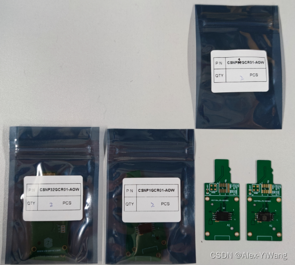
下图是我收到的测试样品:
4 电路结构与接口协议
4.1 SD NAND
本文所使用的产品是CSNP4GCR01-AMW,是雷龙的第二代产品,产品如下图所示:

数据手册可以在立创商城进行下载,其封装与连接的电路原理参考图如下图所示:
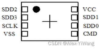
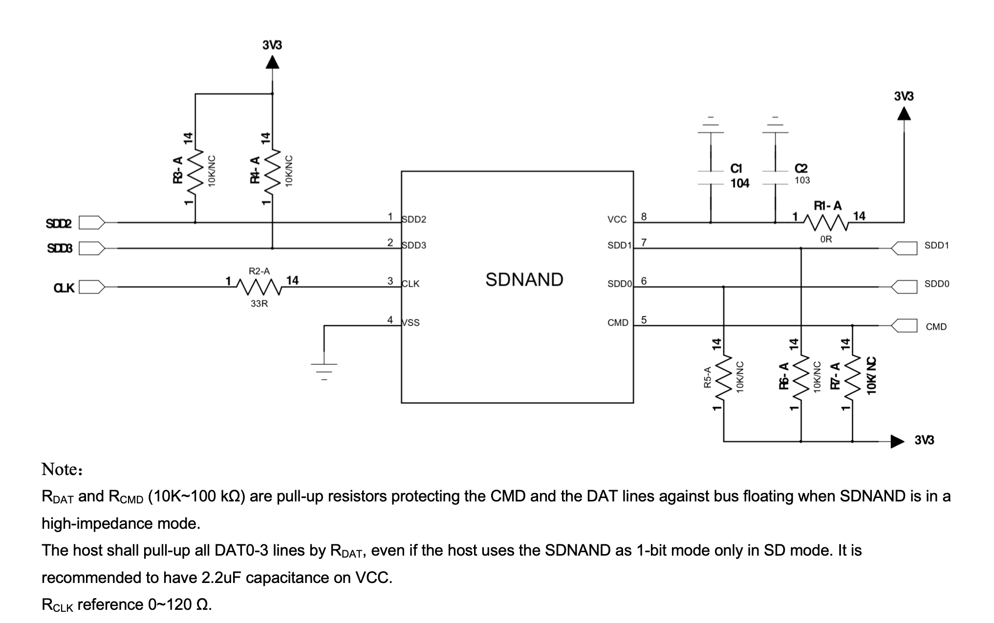
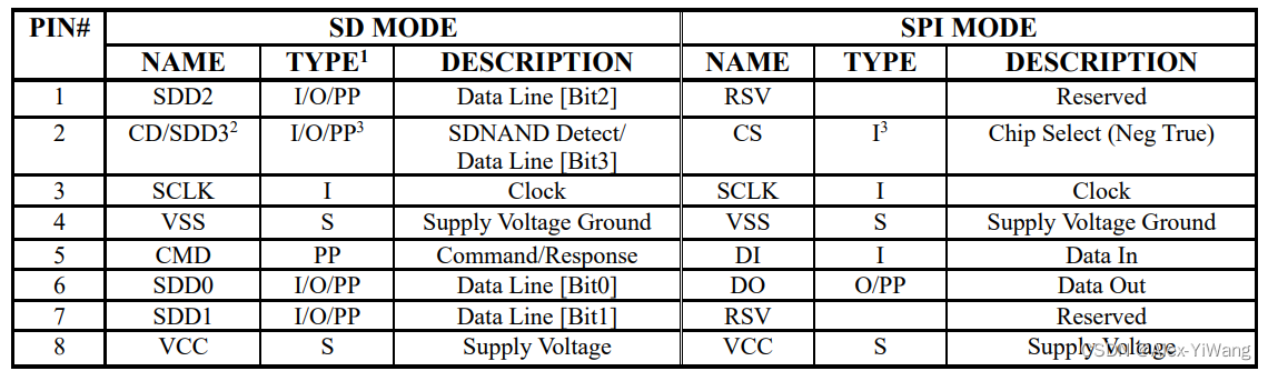
芯片共包含8个引脚,包括4根数据线(6、7、1、2);2根电源线(4、8);1根时钟线(3);1根命令控制线(5)
手册中提供了SD NAND的两种使用模式,分别为SD MODE 以及 SPI MODE。他们所对应的引脚定义,如下图所示:
对于两种模式的切换,官方给出了初始化的方式。下文在代码的时序部分也会涉及到相关内容。
在对SD卡数据读写速度要求不高的情况下,选用SPI通信模式可以说是一种最佳方案。因为在该模式下,同只需要通过四根线就是可以完成所有的数据交换,可以为我们节省出宝贵的FPGA I/O资源。下图给出了SPI一对一通信时,主设备与从设备之间的连接关系。
(注:SPI协议详解传送门)

因此本文主要介绍SPI MODE下各个引脚的功能:
| 引脚 | 功能 |
| CLK | 同步时钟线,与SPI总线时钟SCK相连 |
| CMD | 命令控制线,与SPI总线的MOSI相连,主机用于发送命令 |
| SDD0-3 | 只有SDD0使用,与SPI总线MISO相连,用于主机选择从设备 |
| VCC、VSS | 电源线 |
确定了通讯模式后,也就便于我们后文中,利用这种通讯模式按照SD卡的读写时序进行读写操作。
4.2 SD NAND测试板
单独的SD NAND不便于我们使用FPGA进行读写测试,好在官方提供了测试板,如下图所示:

有了它就可以轻松实现SD NAND与我们常见的FPGA开发板上的Micro SD插槽进行连接与测试了。
适用产品:LGA8,6x8mm 封装的SD NAND产品。
测试板尺寸:长度6.22厘米,宽度2.49厘米,接口长度2.53厘米。
使用方法:将芯片焊接至测试板上,可在原有的Micro SD卡座上直接调试和测试。
准备工具:热风枪,锡膏,镊子。温度要求:将热风枪温度调至300摄氏度℃即可焊接。
4.3 FPGA开发板
本文所使用的是黑金的AX301开发板,上面装有一个 Micro SD 卡座, FPGA 通过 SPI 数据总线访问 Micro SD 卡,SD 卡座和 FPGA 的硬件电路连接如下:
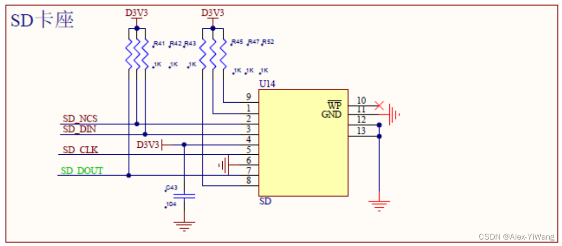
借由硬件电路的连接,FPGA可以直接与我们的SD NAND进行通信了。
至此,我们已经实现了SD NANDSPI通信方式方案的确定以及基于此的硬件电路连接,下一步就是根据SD卡的读写时序讲通信方式初始化为SPI模式,并按照SD卡协议进行读写操作。
5 SD卡协议与时序流程
5.1 SD卡协议
以下内容来自黑金的实验手册:
SD 卡的协议是一种简单的命令/响应的协议。全部命令由主机发起, SD 卡接收到命令后并返
回响应数据。根据命令的不同,返回的数据内容和长度也不同。 SD 卡命令是一个 6 字节组成的命
令包,其中第一个字节为命令号, 命令号高位 bit7 和 bit6 为固定的“01“,其它 6 个 bit 为具体
的命令号。第 2 个字节到第 5 个字节为命令参数。第 6 个字节为 7 个 bit 的 CRC 校验加 1 个 bit 的结束位。 如果在 SPI 模式的时候, CRC 校验位为可选。 如下图所示, Command 表示命令,通常使用十进制表示名称,例如 CMD17,这个时候 Command 就是十进制的 17。
对于详细的SD卡协议内容,可以参考传送门中的相关内容,给出了比较具体的解释。

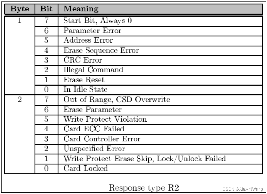
SD 卡对每个命令会返回一个响应,每个命令有一定的响应格式。响应的格式跟给它的命令号
有关。在 SPI 模式中,有三种响应格式: R1, R2, R3。
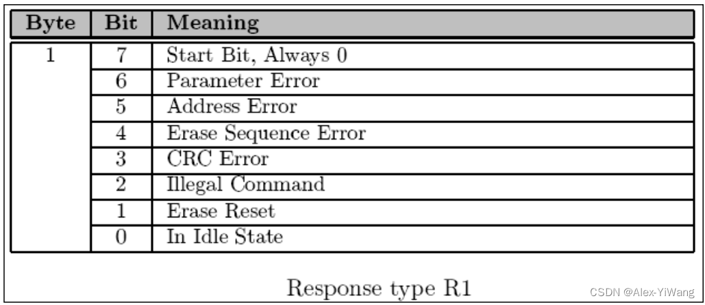

在进行SD NAND的SPI模式读写操作时,主要使用到了以下几种SD卡命令,下面的表格进行简单介绍,这里可以找到完整版:
5.2 SD卡2.0版本初始化步骤
- 上电后延时至少 74clock,等待 SD 卡内部操作完成
- 片选 CS 低电平选中 SD 卡
- 发送 CMD0,需要返回 0x01,进入 Idle 状态
- 为了区别 SD 卡是 2.0 还是 1.0,或是 MMC 卡,这里根据协议向上兼容的,首先发送只有SD2.0 才有的命令 CMD8,如果 CMD8 返回无错误,则初步判断为 2.0 卡,进一步循环发送命令 CMD55+ACMD41,直到返回 0x00,确定 SD2.0 卡
- 如果 CMD8 返回错误则判断为 1.0 卡还是 MMC 卡,循环发送 CMD55+ACMD41,返回无错误,则为 SD1.0 卡,到此 SD1.0 卡初始成功,如果在一定的循环次数下,返回为错误,则进一步发送 CMD1 进行初始化,如果返回无错误,则确定为 MMC 卡,如果在一定的次数下,返回为错误,则不能识别该卡,初始化结束。 (通过 CMD16 可以改变 SD 卡一次性读写的长度)
- CS 拉高
5.3 SD卡的读步骤
- 发送 CMD17(单块)或 CMD18(多块)读命令,返回 0X00
- 接收数据开始令牌 fe(或 fc) +正式数据 512Bytes + CRC 校验 2Bytes(默认正式传输的数据长度是 512Bytes)
5.4 SD卡的写步骤
- 发送 CMD24(单块)或 CMD25(多块)写命令,返回 0X00
- 发送数据开始令牌 fe(或 fc) +正式数据 512Bytes + CRC 校验 2Bytes
6 模块代码
本代码所实现的功能,是基于黑金AX301B,实现对SD NAND FLASH的数据写入与读取,并显示在开发板的数码管上。当按下开发板上的按键时,会自动将数据加一操作,并进行同步显示。
前文介绍的是SD NAND的协议以及初始化、读写操作的流程,下面介绍代码的组成部分,整个工程主要由以下部分模块构成:
sd_card_test(top模块)
ax_debounce:ax_debounce_m0(按键消抖模块)
sd_card_top:sd_card_top_m0(SD卡top模块)
sd_card_cmd:sd_card_cmd_m0(SD卡指令)
sd_card_sec_read_write:sd_card_sec_read_write_m0(SD卡读写)
spi_master:spi_master_m0(SPI一个字节读写)
seg_decoder:seg_decoder_m0(数码管控制)
seg_decoder:seg_decoder_m1(数码管控制)
seg_scan:seg_scan_m0(数码管控制)
下面主要介绍上述四个加粗的模块以及其功能
6.1 sd_card_top
本模块是SD card的top模块,用来实现不同子模块之间的连接。
//
//                                                                              //
//                                                                              //
//  Author: meisq                                                               //
//          msq@qq.com                                                          //
//          ALINX(shanghai) Technology Co.,Ltd                                  //
//          heijin                                                              //
//     WEB: http://www.alinx.cn/                                                //
//     BBS: http://www.heijin.org/                                              //
//                                                                              //
//
//                                                                              //
// Copyright (c) 2017,ALINX(shanghai) Technology Co.,Ltd                        //
//                    All rights reserved                                       //
//                                                                              //
// This source file may be used and distributed without restriction provided    //
// that this copyright statement is not removed from the file and that any      //
// derivative work contains the original copyright notice and the associated    //
// disclaimer.                                                                  //
//                                                                              //
////==========================================================================
//  Revision History:
//  Date          By            Revision    Change Description
//--------------------------------------------------------------------------
//  2017/6/21    meisq         1.0         Original
//*************************************************************************/
module sd_card_top
#(parameter  SPI_LOW_SPEED_DIV = 248,         // SD card low speed mode frequency division parameter,spi clk speed = clk speed /((SPI_LOW_SPEED_DIV + 2) * 2 )parameter  SPI_HIGH_SPEED_DIV = 0           // SD card high speed mode frequency division parameter,spi clk speed = clk speed /((SPI_HIGH_SPEED_DIV + 2) * 2 )
)
(input            clk,input            rst,output           SD_nCS,                    //SD card chip select (SPI mode)output           SD_DCLK,                   //SD card clockoutput           SD_MOSI,                   //SD card controller data outputinput            SD_MISO,                   //SD card controller data inputoutput           sd_init_done,              //SD card initialization is completeinput            sd_sec_read,               //SD card sector readinput[31:0]      sd_sec_read_addr,          //SD card sector read addressoutput[7:0]      sd_sec_read_data,          //SD card sector read dataoutput           sd_sec_read_data_valid,    //SD card sector read data validoutput           sd_sec_read_end,           //SD card sector read endinput            sd_sec_write,              //SD card sector writeinput[31:0]      sd_sec_write_addr,         //SD card sector write addressinput[7:0]       sd_sec_write_data,         //SD card sector write dataoutput           sd_sec_write_data_req,     //SD card sector write data next clock is validoutput           sd_sec_write_end           //SD card sector write end
);
wire[15:0]           spi_clk_div;               //SPI module clock division parameter
wire                 cmd_req;                   //SD card command request
wire                 cmd_req_ack;               //SD card command request response
wire                 cmd_req_error;             //SD card command request error
wire[47:0]           cmd;                       //SD card command
wire[7:0]            cmd_r1;                    //SD card expect response
wire[15:0]           cmd_data_len;              //SD card command read data length
wire                 block_read_req;            //SD card sector data read request
wire                 block_read_valid;          //SD card sector data read data valid
wire[7:0]            block_read_data;           //SD card sector data read data
wire                 block_read_req_ack;        //SD card sector data read response
wire                 block_write_req;           //SD card sector data write request
wire[7:0]            block_write_data;          //SD card sector data write data next clock is valid
wire                 block_write_data_rd;       //SD card sector data write data
wire                 block_write_req_ack;       //SD card sector data write responsewire                 nCS_ctrl;                  //SPI module chip select control
wire                 spi_wr_req;                //SPI module data sending request
wire                 spi_wr_ack;                //SPI module data request response
wire[7:0]            spi_data_in;               //SPI module send data
wire[7:0]            spi_data_out;              //SPI module data returned
wire[15:0]           clk_div;
sd_card_sec_read_write
#(.SPI_LOW_SPEED_DIV(SPI_LOW_SPEED_DIV),.SPI_HIGH_SPEED_DIV(SPI_HIGH_SPEED_DIV)
)
sd_card_sec_read_write_m0(.clk                            (clk                    ),.rst                            (rst                    ),.sd_init_done                   (sd_init_done           ),.sd_sec_read                    (sd_sec_read            ),.sd_sec_read_addr               (sd_sec_read_addr       ),.sd_sec_read_data               (sd_sec_read_data       ),.sd_sec_read_data_valid         (sd_sec_read_data_valid ),.sd_sec_read_end                (sd_sec_read_end        ),.sd_sec_write                   (sd_sec_write           ),.sd_sec_write_addr              (sd_sec_write_addr      ),.sd_sec_write_data              (sd_sec_write_data      ),.sd_sec_write_data_req          (sd_sec_write_data_req  ),.sd_sec_write_end               (sd_sec_write_end       ),.spi_clk_div                    (spi_clk_div            ),.cmd_req                        (cmd_req                ),.cmd_req_ack                    (cmd_req_ack            ),.cmd_req_error                  (cmd_req_error          ),.cmd                            (cmd                    ),.cmd_r1                         (cmd_r1                 ),.cmd_data_len                   (cmd_data_len           ),.block_read_req                 (block_read_req         ),.block_read_valid               (block_read_valid       ),.block_read_data                (block_read_data        ),.block_read_req_ack             (block_read_req_ack     ),.block_write_req                (block_write_req        ),.block_write_data               (block_write_data       ),.block_write_data_rd            (block_write_data_rd    ),.block_write_req_ack            (block_write_req_ack    )
);sd_card_cmd sd_card_cmd_m0(.sys_clk                        (clk                    ),.rst                            (rst                    ),.spi_clk_div                    (spi_clk_div            ),.cmd_req                        (cmd_req                ),.cmd_req_ack                    (cmd_req_ack            ),.cmd_req_error                  (cmd_req_error          ),.cmd                            (cmd                    ),.cmd_r1                         (cmd_r1                 ),.cmd_data_len                   (cmd_data_len           ),.block_read_req                 (block_read_req         ),.block_read_req_ack             (block_read_req_ack     ),.block_read_data                (block_read_data        ),.block_read_valid               (block_read_valid       ),.block_write_req                (block_write_req        ),.block_write_data               (block_write_data       ),.block_write_data_rd            (block_write_data_rd    ),.block_write_req_ack            (block_write_req_ack    ),.nCS_ctrl                       (nCS_ctrl               ),.clk_div                        (clk_div                ),.spi_wr_req                     (spi_wr_req             ),.spi_wr_ack                     (spi_wr_ack             ),.spi_data_in                    (spi_data_in            ),.spi_data_out                   (spi_data_out           ));spi_master spi_master_m0(.sys_clk                        (clk                    ),.rst                            (rst                    ),.nCS                            (SD_nCS                 ),.DCLK                           (SD_DCLK                ),.MOSI                           (SD_MOSI                ),.MISO                           (SD_MISO                ),.clk_div                        (clk_div                ),.CPOL                           (1'b1                   ),.CPHA                           (1'b1                   ),.nCS_ctrl                       (nCS_ctrl               ),.wr_req                         (spi_wr_req             ),.wr_ack                         (spi_wr_ack             ),.data_in                        (spi_data_in            ),.data_out                       (spi_data_out           )
);
endmodule
6.2 sd_card_cmd
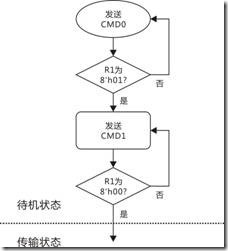
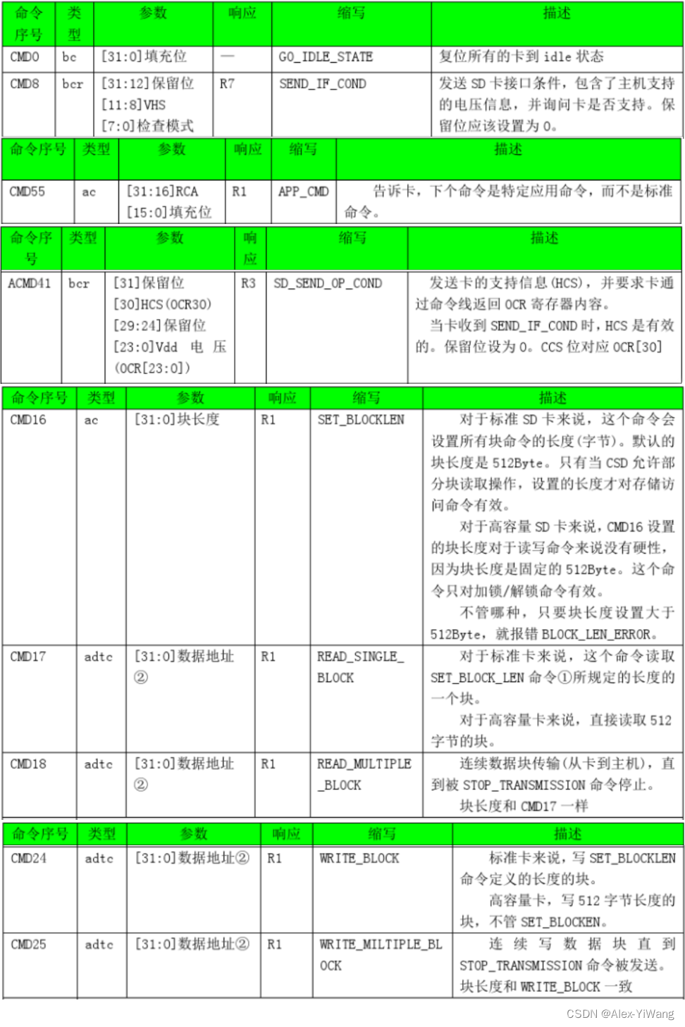
sd_card_cmd 模块主要实验 sd 卡基本命令操作,还有上电初始化的 88 个周期的时钟,数据
块的读写,状态机如下:
代码如下:
//
//                                                                              //
//                                                                              //
//  Author: meisq                                                               //
//          msq@qq.com                                                          //
//          ALINX(shanghai) Technology Co.,Ltd                                  //
//          heijin                                                              //
//     WEB: http://www.alinx.cn/                                                //
//     BBS: http://www.heijin.org/                                              //
//                                                                              //
//
//                                                                              //
// Copyright (c) 2017,ALINX(shanghai) Technology Co.,Ltd                        //
//                    All rights reserved                                       //
//                                                                              //
// This source file may be used and distributed without restriction provided    //
// that this copyright statement is not removed from the file and that any      //
// derivative work contains the original copyright notice and the associated    //
// disclaimer.                                                                  //
//                                                                              //
////==========================================================================
//  Revision History:
//  Date          By            Revision    Change Description
//--------------------------------------------------------------------------
//  2017/6/21     meisq         1.0         Original
//*************************************************************************/
module sd_card_cmd(input                       sys_clk,input                       rst,input[15:0]                 spi_clk_div,                  //SPI module clock division parameterinput                       cmd_req,                      //SD card command requestoutput                      cmd_req_ack,                  //SD card command request responseoutput reg                  cmd_req_error,                //SD card command request errorinput[47:0]                 cmd,                          //SD card commandinput[7:0]                  cmd_r1,                       //SD card expect responseinput[15:0]                 cmd_data_len,                 //SD card command read data lengthinput                       block_read_req,               //SD card sector data read requestoutput reg                  block_read_valid,             //SD card sector data read data validoutput reg[7:0]             block_read_data,              //SD card sector data read dataoutput                      block_read_req_ack,           //SD card sector data read responseinput                       block_write_req,              //SD card sector data write requestinput[7:0]                  block_write_data,             //SD card sector data write data next clock is validoutput                      block_write_data_rd,          //SD card sector data write dataoutput                      block_write_req_ack,          //SD card sector data write responseoutput                      nCS_ctrl,                     //SPI module chip select controloutput reg[15:0]            clk_div,output reg                  spi_wr_req,                   //SPI module data sending requestinput                       spi_wr_ack,                   //SPI module data request responseoutput[7:0]                 spi_data_in,                  //SPI module send datainput[7:0]                  spi_data_out                  //SPI module data returned
);
parameter S_IDLE         = 0;
parameter S_WAIT         = 1;
parameter S_INIT         = 2;
parameter S_CMD_PRE      = 3;
parameter S_CMD          = 4;
parameter S_CMD_DATA     = 5;
parameter S_READ_WAIT    = 6;
parameter S_READ         = 7;
parameter S_READ_ACK     = 8;
parameter S_WRITE_TOKEN  = 9;
parameter S_WRITE_DATA_0 = 10;
parameter S_WRITE_DATA_1 = 11;
parameter S_WRITE_CRC    = 12;
parameter S_WRITE_ACK    = 13;
parameter S_ERR          = 14;
parameter S_END          = 15;reg[3:0]                      state;
reg                           CS_reg;
reg[15:0]                     byte_cnt;
reg[7:0]                      send_data;
wire[7:0]                     data_recv;
reg[9:0]                      wr_data_cnt;assign cmd_req_ack = (state == S_END);
assign block_read_req_ack = (state == S_READ_ACK);
assign block_write_req_ack= (state == S_WRITE_ACK);
assign block_write_data_rd = (state == S_WRITE_DATA_0);
assign spi_data_in = send_data;
assign data_recv = spi_data_out;
assign nCS_ctrl = CS_reg;
always@(posedge sys_clk or posedge rst)
beginif(rst == 1'b1)beginCS_reg <= 1'b1;spi_wr_req <= 1'b0;byte_cnt <= 16'd0;clk_div <= 16'd0;send_data <= 8'hff;state <= S_IDLE;cmd_req_error <= 1'b0;wr_data_cnt <= 10'd0;endelsecase(state)S_IDLE:beginstate <= S_INIT;clk_div <= spi_clk_div;CS_reg <= 1'b1;endS_INIT:begin//send 11 bytes on power(at least 74 SPI clocks)if(spi_wr_ack == 1'b1)beginif(byte_cnt >= 16'd10)beginbyte_cnt <= 16'd0;spi_wr_req <= 1'b0;state <= S_WAIT;endbeginbyte_cnt <= byte_cnt + 16'd1;endendelsebeginspi_wr_req <= 1'b1;send_data <= 8'hff;endendS_WAIT:begincmd_req_error <= 1'b0;wr_data_cnt <= 10'd0;//wait for  instructionif(cmd_req == 1'b1)state <= S_CMD_PRE;else if(block_read_req == 1'b1)state <= S_READ_WAIT;else if(block_write_req == 1'b1)state <= S_WRITE_TOKEN;clk_div <= spi_clk_div;endS_CMD_PRE:begin//before sending a command, send an byte 'ff',provide some clocksif(spi_wr_ack == 1'b1)beginstate <= S_CMD;spi_wr_req <= 1'b0;byte_cnt <= 16'd0;endelsebeginspi_wr_req <= 1'b1;CS_reg <= 1'b1;send_data <= 8'hff;endendS_CMD:beginif(spi_wr_ack == 1'b1)beginif((byte_cnt == 16'hffff) || (data_recv != cmd_r1 && data_recv[7] == 1'b0))beginstate <= S_ERR;spi_wr_req <= 1'b0;endelse if(data_recv == cmd_r1)beginspi_wr_req <= 1'b0;if(cmd_data_len != 16'd0)beginstate <= S_CMD_DATA;byte_cnt <= 16'd0;endelsestate <= S_END;endelsebyte_cnt <=  byte_cnt + 16'd1;endelsebeginspi_wr_req <= 1'b1;CS_reg <= 1'b0;if(byte_cnt == 16'd0)send_data <= (cmd[47:40] | 8'h40);else if(byte_cnt == 16'd1)send_data <= cmd[39:32];else if(byte_cnt == 16'd2)send_data <= cmd[31:24];else if(byte_cnt == 16'd3)send_data <= cmd[23:16];else if(byte_cnt == 16'd4)send_data <= cmd[15:8];else if(byte_cnt == 16'd5)send_data <= cmd[7:0];elsesend_data <= 8'hff;endendS_CMD_DATA:beginif(spi_wr_ack == 1'b1)beginif(byte_cnt == cmd_data_len - 16'd1)beginstate <= S_END;spi_wr_req <= 1'b0;byte_cnt <= 16'd0;endelsebeginbyte_cnt <= byte_cnt + 16'd1;endendelsebeginspi_wr_req <= 1'b1;send_data <= 8'hff;endendS_READ_WAIT:beginif(spi_wr_ack == 1'b1 && data_recv == 8'hfe)beginspi_wr_req <= 1'b0;state <= S_READ;byte_cnt <= 16'd0;endelsebeginspi_wr_req <= 1'b1;send_data <= 8'hff;endendS_READ:beginif(spi_wr_ack == 1'b1)beginif(byte_cnt == 16'd513)beginstate <= S_READ_ACK;spi_wr_req <= 1'b0;byte_cnt <= 16'd0;endelsebeginbyte_cnt <= byte_cnt + 16'd1;endendelsebeginspi_wr_req <= 1'b1;send_data <= 8'hff;endendS_WRITE_TOKEN:if(spi_wr_ack == 1'b1)beginstate <= S_WRITE_DATA_0;spi_wr_req <= 1'b0;endelsebeginspi_wr_req <= 1'b1;send_data <= 8'hfe;endS_WRITE_DATA_0:beginstate <= S_WRITE_DATA_1;wr_data_cnt <= wr_data_cnt + 10'd1;endS_WRITE_DATA_1:beginif(spi_wr_ack == 1'b1 && wr_data_cnt == 10'd512)beginstate <= S_WRITE_CRC;spi_wr_req <= 1'b0;endelse if(spi_wr_ack == 1'b1)beginstate <= S_WRITE_DATA_0;spi_wr_req <= 1'b0;endelsebeginspi_wr_req <= 1'b1;send_data <= block_write_data;endendS_WRITE_CRC:beginif(spi_wr_ack == 1'b1)beginif(byte_cnt == 16'd2)beginstate <= S_WRITE_ACK;spi_wr_req <= 1'b0;byte_cnt <= 16'd0;endelsebeginbyte_cnt <= byte_cnt + 16'd1;endendelsebeginspi_wr_req <= 1'b1;send_data <= 8'hff;endendS_ERR:beginstate <= S_END;cmd_req_error <= 1'b1;endS_READ_ACK,S_WRITE_ACK,S_END:beginstate <= S_WAIT;enddefault:state <= S_IDLE;endcase
end
always@(posedge sys_clk or posedge rst)
beginif(rst == 1'b1)block_read_valid <= 1'b0;else if(state == S_READ && byte_cnt < 16'd512)block_read_valid <= spi_wr_ack;elseblock_read_valid <= 1'b0;
endalways@(posedge sys_clk or posedge rst)
beginif(rst == 1'b1)block_read_data <= 8'd0;else if(state == S_READ && spi_wr_ack == 1'b1)block_read_data <= data_recv;
endendmodule
6.3 sd_card_sec_read_write
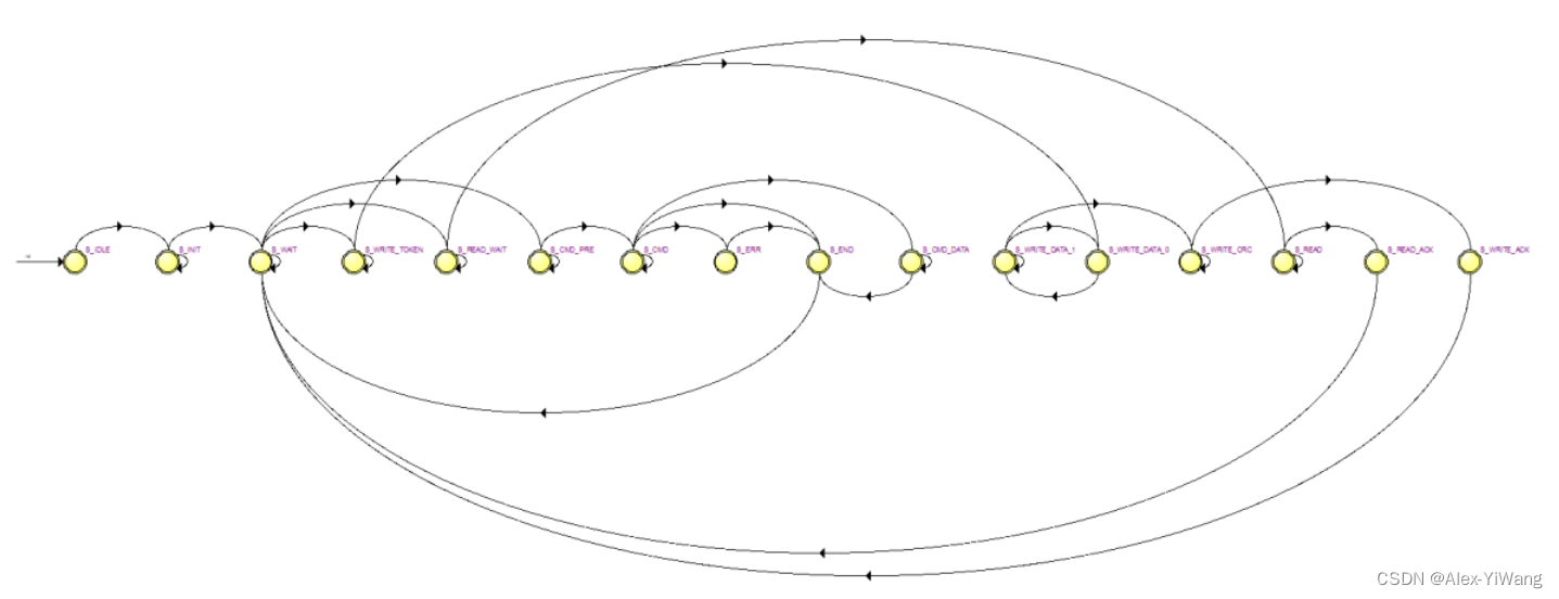
sd_card_sec_read_write 模块继续完成 SD 卡初始化,然后等待扇区读写指令,并完成扇区的
读写操作。 下图为模块的状态机转换图,首先发送 CMD0 命令,然后发送 CMD8 命令,再发送
CMD55,接着发送 ACMD41,如果应答正常, sd 卡初始化完成,等待扇区的读写。

代码如下:
//
//                                                                              //
//                                                                              //
//  Author: meisq                                                               //
//          msq@qq.com                                                          //
//          ALINX(shanghai) Technology Co.,Ltd                                  //
//          heijin                                                              //
//     WEB: http://www.alinx.cn/                                                //
//     BBS: http://www.heijin.org/                                              //
//                                                                              //
//
//                                                                              //
// Copyright (c) 2017,ALINX(shanghai) Technology Co.,Ltd                        //
//                    All rights reserved                                       //
//                                                                              //
// This source file may be used and distributed without restriction provided    //
// that this copyright statement is not removed from the file and that any      //
// derivative work contains the original copyright notice and the associated    //
// disclaimer.                                                                  //
//                                                                              //
////===============================================================================
//  Revision History:
//  Date          By            Revision    Change Description
//-------------------------------------------------------------------------------
//  2017/6/21     meisq         1.0         Original
//*******************************************************************************/
module sd_card_sec_read_write
#(parameter  SPI_LOW_SPEED_DIV = 248,         // spi clk speed = clk speed /((SPI_LOW_SPEED_DIV + 2) * 2 )parameter  SPI_HIGH_SPEED_DIV = 0           // spi clk speed = clk speed /((SPI_HIGH_SPEED_DIV + 2) * 2 )
)
(input            clk,input            rst,output reg       sd_init_done,input            sd_sec_read,input[31:0]      sd_sec_read_addr,output[7:0]      sd_sec_read_data,output           sd_sec_read_data_valid,output           sd_sec_read_end,input            sd_sec_write,input[31:0]      sd_sec_write_addr,input[7:0]       sd_sec_write_data,output           sd_sec_write_data_req,output           sd_sec_write_end,output reg[15:0] spi_clk_div,output reg       cmd_req,input            cmd_req_ack,input            cmd_req_error,output reg[47:0] cmd,output reg[7:0]  cmd_r1,output reg[15:0] cmd_data_len,output reg       block_read_req,input            block_read_valid,input[7:0]       block_read_data,input            block_read_req_ack,output reg       block_write_req,output[7:0]      block_write_data,input            block_write_data_rd,input            block_write_req_ack
);
reg[7:0] read_data;
reg[31:0] timer;localparam S_IDLE               = 0;
localparam S_CMD0               = 1;
localparam S_CMD8               = 2;
localparam S_CMD55              = 3;
localparam S_CMD41              = 4;
localparam S_CMD17              = 5;
localparam S_READ               = 6;
localparam S_CMD24              = 7;
localparam S_WRITE              = 8;
localparam S_ERR                = 14;
localparam S_WRITE_END          = 15;
localparam S_READ_END           = 16;
localparam S_WAIT_READ_WRITE    = 17;
localparam S_CMD16              = 18;reg[4:0]                       state;
reg[31:0]                      sec_addr;
assign sd_sec_read_data_valid = (state == S_READ) && block_read_valid;
assign sd_sec_read_data = block_read_data;
assign sd_sec_read_end = (state == S_READ_END);
assign sd_sec_write_data_req = (state == S_WRITE) && block_write_data_rd;
assign block_write_data = sd_sec_write_data;
assign sd_sec_write_end = (state == S_WRITE_END);always@(posedge clk or posedge rst)
beginif(rst == 1'b1)beginstate <= S_IDLE;cmd_req <= 1'b0;cmd_data_len <= 16'd0;cmd_r1 <= 8'd0;cmd <= 48'd0;spi_clk_div <= SPI_LOW_SPEED_DIV[15:0];block_write_req <= 1'b0;block_read_req <= 1'b0;sec_addr <= 32'd0;sd_init_done <= 1'b0;endelsecase(state)S_IDLE:beginstate <= S_CMD0;sd_init_done <= 1'b0;spi_clk_div <= SPI_LOW_SPEED_DIV[15:0];endS_CMD0:beginif(cmd_req_ack & ~cmd_req_error)beginstate <= S_CMD8;cmd_req <= 1'b0;endelsebegincmd_req <= 1'b1;cmd_data_len <= 16'd0;cmd_r1 <= 8'h01;cmd <= {8'd0,8'h00,8'h00,8'h00,8'h00,8'h95};endendS_CMD8:beginif(cmd_req_ack & ~cmd_req_error)beginstate <= S_CMD55;cmd_req <= 1'b0;endelsebegincmd_req <= 1'b1;cmd_data_len <= 16'd4;cmd_r1 <= 8'h01;cmd <= {8'd8,8'h00,8'h00,8'h01,8'haa,8'h87};endendS_CMD55:beginif(cmd_req_ack & ~cmd_req_error)beginstate <= S_CMD41;cmd_req <= 1'b0;endelsebegincmd_req <= 1'b1;cmd_data_len <= 16'd0;cmd_r1 <= 8'h01;cmd <= {8'd55,8'h00,8'h00,8'h00,8'h00,8'hff};endendS_CMD41:beginif(cmd_req_ack & ~cmd_req_error)beginstate <= S_CMD16;cmd_req <= 1'b0;sd_init_done <= 1'b1;spi_clk_div <= SPI_HIGH_SPEED_DIV[15:0];endelse if(cmd_req_ack)beginstate <= S_CMD55;endelsebegincmd_req <= 1'b1;cmd_data_len <= 16'd0;cmd_r1 <= 8'h00;cmd <= {8'd41,8'h40,8'h00,8'h00,8'h00,8'hff};endendS_CMD16:beginif(cmd_req_ack & ~cmd_req_error)beginstate <= S_WAIT_READ_WRITE;cmd_req <= 1'b0;sd_init_done <= 1'b1;spi_clk_div <= SPI_HIGH_SPEED_DIV[15:0];endelse if(cmd_req_ack)beginstate <= S_CMD55;endelsebegincmd_req <= 1'b1;cmd_data_len <= 16'd0;cmd_r1 <= 8'h00;cmd <= {8'd16,32'd512,8'hff};endend			S_WAIT_READ_WRITE:beginif(sd_sec_write ==  1'b1)beginstate <= S_CMD24;sec_addr <= sd_sec_write_addr;endelse if(sd_sec_read == 1'b1)beginstate <= S_CMD17;sec_addr <= sd_sec_read_addr;endspi_clk_div <= 16'd0;endS_CMD24:beginif(cmd_req_ack & ~cmd_req_error)beginstate <= S_WRITE;cmd_req <= 1'b0;endelsebegincmd_req <= 1'b1;cmd_data_len <= 16'd0;cmd_r1 <= 8'h00;cmd <= {8'd24,sec_addr,8'hff};endendS_WRITE:beginif(block_write_req_ack == 1'b1)beginblock_write_req <= 1'b0;state <= S_WRITE_END;endelseblock_write_req <= 1'b1;endS_CMD17:beginif(cmd_req_ack & ~cmd_req_error)beginstate <= S_READ;cmd_req <= 1'b0;endelsebegincmd_req <= 1'b1;cmd_data_len <= 16'd0;cmd_r1 <= 8'h00;cmd <= {8'd17,sec_addr,8'hff};endendS_READ:beginif(block_read_req_ack)beginstate <= S_READ_END;block_read_req <= 1'b0;endelsebeginblock_read_req <= 1'b1;endendS_WRITE_END:beginstate <= S_WAIT_READ_WRITE;endS_READ_END:beginstate <= S_WAIT_READ_WRITE;enddefault:state <= S_IDLE;endcase
end
endmodule
6.4 spi_master
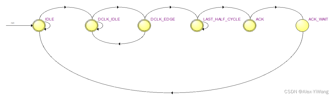
这一模块用来完成SPI一个字节的读写。
spi master 状态机设计, 主要完成一个字节 spi 数据的读写,由于是全双工的,写一个字节的
同时也读一个字节。 首先空闲状态“IDLE”接收到写请求后进入“DCLK_IDLE”状态,这个状态为
spi 时钟沿变化保持一定的时间,用来控制 spi 时钟的周期,然后进入 spi 时钟沿的变化状态,一
个字节上升沿和下降沿一共 16 个数据沿。 在最后一个数据沿进入“LAST_HALF_CYCLE”状态,为
让最后一个沿也保持一定的时间,再进入应答状态,完成一次写请求。spi_master 模块中模拟了一个 spi 时钟,在状态机进入到‘DCLK_EDGE’时进行翻转。状态机图示如下:
代码如下:
//
//                                                                              //
//                                                                              //
//  Author: meisq                                                               //
//          msq@qq.com                                                          //
//          ALINX(shanghai) Technology Co.,Ltd                                  //
//          heijin                                                              //
//     WEB: http://www.alinx.cn/                                                //
//     BBS: http://www.heijin.org/                                              //
//                                                                              //
//
//                                                                              //
// Copyright (c) 2017,ALINX(shanghai) Technology Co.,Ltd                        //
//                    All rights reserved                                       //
//                                                                              //
// This source file may be used and distributed without restriction provided    //
// that this copyright statement is not removed from the file and that any      //
// derivative work contains the original copyright notice and the associated    //
// disclaimer.                                                                  //
//                                                                              //
////==========================================================================
//  Revision History:
//  Date          By            Revision    Change Description
//--------------------------------------------------------------------------
//  2017/6/19     meisq         1.0         Original
//*************************************************************************/
module spi_master
(input                       sys_clk,input                       rst,output                      nCS,       //chip select (SPI mode)output                      DCLK,      //spi clockoutput                      MOSI,      //spi data outputinput                       MISO,      //spi inputinput                       CPOL,input                       CPHA,input                       nCS_ctrl,input[15:0]                 clk_div,input                       wr_req,output                      wr_ack,input[7:0]                  data_in,output[7:0]                 data_out
);
localparam                   IDLE            = 0;
localparam                   DCLK_EDGE       = 1;
localparam                   DCLK_IDLE       = 2;
localparam                   ACK             = 3;
localparam                   LAST_HALF_CYCLE = 4;
localparam                   ACK_WAIT        = 5;
reg                          DCLK_reg;
reg[7:0]                     MOSI_shift;
reg[7:0]                     MISO_shift;
reg[2:0]                     state;
reg[2:0]                     next_state;
reg [15:0]                   clk_cnt;
reg[4:0]                     clk_edge_cnt;
assign MOSI = MOSI_shift[7];
assign DCLK = DCLK_reg;
assign data_out = MISO_shift;
assign wr_ack = (state == ACK);
assign nCS = nCS_ctrl;
always@(posedge sys_clk or posedge rst)
beginif(rst)state <= IDLE;elsestate <= next_state;
endalways@(*)
begincase(state)IDLE:if(wr_req == 1'b1)next_state <= DCLK_IDLE;elsenext_state <= IDLE;DCLK_IDLE://half a SPI clock cycle produces a clock edgeif(clk_cnt == clk_div)next_state <= DCLK_EDGE;elsenext_state <= DCLK_IDLE;DCLK_EDGE://a SPI byte with a total of 16 clock edgesif(clk_edge_cnt == 5'd15)next_state <= LAST_HALF_CYCLE;elsenext_state <= DCLK_IDLE;//this is the last data edgeLAST_HALF_CYCLE:if(clk_cnt == clk_div)next_state <= ACK;elsenext_state <= LAST_HALF_CYCLE;//send one byte completeACK:next_state <= ACK_WAIT;//wait for one clock cycle, to ensure that the cancel request signalACK_WAIT:next_state <= IDLE;default:next_state <= IDLE;endcase
endalways@(posedge sys_clk or posedge rst)
beginif(rst)DCLK_reg <= 1'b0;else if(state == IDLE)DCLK_reg <= CPOL;else if(state == DCLK_EDGE)DCLK_reg <= ~DCLK_reg;//SPI clock edge
end
//SPI clock wait counter
always@(posedge sys_clk or posedge rst)
beginif(rst)clk_cnt <= 16'd0;else if(state == DCLK_IDLE || state == LAST_HALF_CYCLE)clk_cnt <= clk_cnt + 16'd1;elseclk_cnt <= 16'd0;
end
//SPI clock edge counter
always@(posedge sys_clk or posedge rst)
beginif(rst)clk_edge_cnt <= 5'd0;else if(state == DCLK_EDGE)clk_edge_cnt <= clk_edge_cnt + 5'd1;else if(state == IDLE)clk_edge_cnt <= 5'd0;
end
//SPI data output
always@(posedge sys_clk or posedge rst)
beginif(rst)MOSI_shift <= 8'd0;else if(state == IDLE && wr_req)MOSI_shift <= data_in;else if(state == DCLK_EDGE)if(CPHA == 1'b0 && clk_edge_cnt[0] == 1'b1)MOSI_shift <= {MOSI_shift[6:0],MOSI_shift[7]};else if(CPHA == 1'b1 && (clk_edge_cnt != 5'd0 && clk_edge_cnt[0] == 1'b0))MOSI_shift <= {MOSI_shift[6:0],MOSI_shift[7]};
end
//SPI data input
always@(posedge sys_clk or posedge rst)
beginif(rst)MISO_shift <= 8'd0;else if(state == IDLE && wr_req)MISO_shift <= 8'h00;else if(state == DCLK_EDGE)if(CPHA == 1'b0 && clk_edge_cnt[0] == 1'b0)MISO_shift <= {MISO_shift[6:0],MISO};else if(CPHA == 1'b1 && (clk_edge_cnt[0] == 1'b1))MISO_shift <= {MISO_shift[6:0],MISO};
end
endmodule
6.5 其余代码
6.5.1 sd_card_test
//
//                                                                              //
//                                                                              //
//  Author: meisq                                                               //
//          msq@qq.com                                                          //
//          ALINX(shanghai) Technology Co.,Ltd                                  //
//          heijin                                                              //
//     WEB: http://www.alinx.cn/                                                //
//     BBS: http://www.heijin.org/                                              //
//                                                                              //
//
//                                                                              //
// Copyright (c) 2017,ALINX(shanghai) Technology Co.,Ltd                        //
//                    All rights reserved                                       //
//                                                                              //
// This source file may be used and distributed without restriction provided    //
// that this copyright statement is not removed from the file and that any      //
// derivative work contains the original copyright notice and the associated    //
// disclaimer.                                                                  //
//                                                                              //
////================================================================================
//  Revision History:
//  Date          By            Revision    Change Description
//--------------------------------------------------------------------------------
//  2017/6/19     meisq         1.0         Original
//*******************************************************************************/
module sd_card_test(input            clk,input            rst_n,input            key1,output           SD_nCS,output           SD_DCLK,output           SD_MOSI,input            SD_MISO,output [5:0]     seg_sel,output [7:0]     seg_data
);
parameter S_IDLE         = 0;
parameter S_READ         = 1;
parameter S_WRITE        = 2;
parameter S_END          = 3;reg[3:0] state;
wire             sd_init_done;
reg              sd_sec_read;
wire[31:0]       sd_sec_read_addr;
wire[7:0]        sd_sec_read_data;
wire             sd_sec_read_data_valid;
wire             sd_sec_read_end;
reg              sd_sec_write;
wire[31:0]       sd_sec_write_addr;
reg [7:0]        sd_sec_write_data;
wire             sd_sec_write_data_req;
wire             sd_sec_write_end;
reg[9:0]         wr_cnt;
reg[9:0]         rd_cnt;
wire             button_negedge;
reg[7:0]         read_data;
ax_debounce ax_debounce_m0
(.clk             (clk),.rst             (~rst_n),.button_in       (key1),.button_posedge  (),.button_negedge  (button_negedge),.button_out      ()
);wire[6:0] seg_data_0;
seg_decoder seg_decoder_m0(.bin_data  (read_data[3:0]),.seg_data  (seg_data_0)
);
wire[6:0] seg_data_1;
seg_decoder seg_decoder_m1(.bin_data  (read_data[7:4]),.seg_data  (seg_data_1)
);
seg_scan seg_scan_m0(.clk        (clk),.rst_n      (rst_n),.seg_sel    (seg_sel),.seg_data   (seg_data),.seg_data_0 ({1'b1,7'b1111_111}),.seg_data_1 ({1'b1,7'b1111_111}),.seg_data_2 ({1'b1,7'b1111_111}),.seg_data_3 ({1'b1,7'b1111_111}),.seg_data_4 ({1'b1,seg_data_1}),.seg_data_5 ({sd_init_done,seg_data_0})
);always@(posedge clk or negedge rst_n)
beginif(rst_n == 1'b0)wr_cnt <= 10'd0;else if(state == S_WRITE)beginif(sd_sec_write_data_req == 1'b1)wr_cnt <= wr_cnt + 10'd1;endelsewr_cnt <= 10'd0;
endalways@(posedge clk or negedge rst_n)
beginif(rst_n == 1'b0)rd_cnt <= 10'd0;else if(state == S_READ)beginif(sd_sec_read_data_valid == 1'b1)rd_cnt <= rd_cnt + 10'd1;endelserd_cnt <= 10'd0;
endalways@(posedge clk or negedge rst_n)
beginif(rst_n == 1'b0)read_data <= 8'd0;else if(state == S_READ)beginif(sd_sec_read_data_valid == 1'b1 && rd_cnt == 10'd0)read_data <= sd_sec_read_data;endelse if(state == S_END && button_negedge == 1'b1)read_data <= read_data + 8'd1;
endalways@(posedge clk or negedge rst_n)
beginif(rst_n == 1'b0)sd_sec_write_data <= 8'd0;else if(sd_sec_write_data_req)sd_sec_write_data <= read_data + wr_cnt[7:0];
endalways@(posedge clk or negedge rst_n)
beginif(rst_n == 1'b0)beginstate <= S_IDLE;sd_sec_read <= 1'b0;sd_sec_write <= 1'b0;endelse if(sd_init_done == 1'b0)beginstate <= S_IDLE;endelsecase(state)S_IDLE:beginstate <= S_READ;endS_WRITE:beginif(sd_sec_write_end == 1'b1)beginsd_sec_write <= 1'b0;state <= S_READ;endelsesd_sec_write <= 1'b1;endS_READ:beginif(sd_sec_read_end == 1'b1)beginstate <= S_END;sd_sec_read <= 1'b0;endelsebeginsd_sec_read <= 1'b1;end                 end         S_END:beginif(button_negedge == 1'b1)state <= S_WRITE;enddefault:state <= S_IDLE;endcase
endsd_card_top  sd_card_top_m0(.clk                       (clk                    ),.rst                       (~rst_n                 ),.SD_nCS                    (SD_nCS                 ),.SD_DCLK                   (SD_DCLK                ),.SD_MOSI                   (SD_MOSI                ),.SD_MISO                   (SD_MISO                ),.sd_init_done              (sd_init_done           ),.sd_sec_read               (sd_sec_read            ),.sd_sec_read_addr          (sd_sec_read_addr       ),.sd_sec_read_data          (sd_sec_read_data       ),.sd_sec_read_data_valid    (sd_sec_read_data_valid ),.sd_sec_read_end           (sd_sec_read_end        ),.sd_sec_write              (sd_sec_write           ),.sd_sec_write_addr         (sd_sec_write_addr      ),.sd_sec_write_data         (sd_sec_write_data      ),.sd_sec_write_data_req     (sd_sec_write_data_req  ),.sd_sec_write_end          (sd_sec_write_end       )
);
endmodule
6.5.2 ax_debounce
//
//                                                                              //
//                                                                              //
//  Author: meisq                                                               //
//          msq@qq.com                                                          //
//          ALINX(shanghai) Technology Co.,Ltd                                  //
//          heijin                                                              //
//     WEB: http://www.alinx.cn/                                                //
//     BBS: http://www.heijin.org/                                              //
//                                                                              //
//
//                                                                              //
// Copyright (c) 2017,ALINX(shanghai) Technology Co.,Ltd                        //
//                    All rights reserved                                       //
//                                                                              //
// This source file may be used and distributed without restriction provided    //
// that this copyright statement is not removed from the file and that any      //
// derivative work contains the original copyright notice and the associated    //
// disclaimer.                                                                  //
//                                                                              //
////================================================================================
//  Revision History:
//  Date          By            Revision    Change Description
//--------------------------------------------------------------------------------
//  2017/5/3     meisq          1.0         Original
//*******************************************************************************/`timescale 1 ns / 100 ps
module  ax_debounce
(input       clk, input       rst, input       button_in,output reg  button_posedge,output reg  button_negedge,output reg  button_out
);---------------- internal constants --------------
parameter N = 32 ;           // debounce timer bitwidth
parameter FREQ = 50;         //model clock :Mhz
parameter MAX_TIME = 20;     //ms
localparam TIMER_MAX_VAL =   MAX_TIME * 1000 * FREQ;
---------------- internal variables ---------------
reg  [N-1 : 0]  q_reg;      // timing regs
reg  [N-1 : 0]  q_next;
reg DFF1, DFF2;             // input flip-flops
wire q_add;                 // control flags
wire q_reset;
reg button_out_d0;------------------------------------------------------contenious assignment for counter control
assign q_reset = (DFF1  ^ DFF2);          // xor input flip flops to look for level chage to reset counter
assign q_add = ~(q_reg == TIMER_MAX_VAL); // add to counter when q_reg msb is equal to 0combo counter to manage q_next
always @ ( q_reset, q_add, q_reg)
begincase( {q_reset , q_add})2'b00 :q_next <= q_reg;2'b01 :q_next <= q_reg + 1;default :q_next <= { N {1'b0} };endcase
endFlip flop inputs and q_reg update
always @ ( posedge clk or posedge rst)
beginif(rst == 1'b1)beginDFF1 <= 1'b0;DFF2 <= 1'b0;q_reg <= { N {1'b0} };endelsebeginDFF1 <= button_in;DFF2 <= DFF1;q_reg <= q_next;end
endcounter control
always @ ( posedge clk or posedge rst)
beginif(rst == 1'b1)button_out <= 1'b1;else if(q_reg == TIMER_MAX_VAL)button_out <= DFF2;elsebutton_out <= button_out;
endalways @ ( posedge clk or posedge rst)
beginif(rst == 1'b1)beginbutton_out_d0 <= 1'b1;button_posedge <= 1'b0;button_negedge <= 1'b0;endelsebeginbutton_out_d0 <= button_out;button_posedge <= ~button_out_d0 & button_out;button_negedge <= button_out_d0 & ~button_out;end
end
endmodule
6.5.3 seg_decoder
//
//                                                                              //
//                                                                              //
//  Author: meisq                                                               //
//          msq@qq.com                                                          //
//          ALINX(shanghai) Technology Co.,Ltd                                  //
//          heijin                                                              //
//     WEB: http://www.alinx.cn/                                                //
//     BBS: http://www.heijin.org/                                              //
//                                                                              //
//
//                                                                              //
// Copyright (c) 2017,ALINX(shanghai) Technology Co.,Ltd                        //
//                    All rights reserved                                       //
//                                                                              //
// This source file may be used and distributed without restriction provided    //
// that this copyright statement is not removed from the file and that any      //
// derivative work contains the original copyright notice and the associated    //
// disclaimer.                                                                  //
//                                                                              //
////==========================================================================
//  Revision History:
//  Date          By            Revision    Change Description
//--------------------------------------------------------------------------
//  2017/6/19     meisq         1.0         Original
//*************************************************************************/
module seg_decoder
(input[3:0]      bin_data,     // bin data inputoutput reg[6:0] seg_data      // seven segments LED output
);always@(*)
begincase(bin_data)4'd0:seg_data <= 7'b100_0000;4'd1:seg_data <= 7'b111_1001;4'd2:seg_data <= 7'b010_0100;4'd3:seg_data <= 7'b011_0000;4'd4:seg_data <= 7'b001_1001;4'd5:seg_data <= 7'b001_0010;4'd6:seg_data <= 7'b000_0010;4'd7:seg_data <= 7'b111_1000;4'd8:seg_data <= 7'b000_0000;4'd9:seg_data <= 7'b001_0000;4'ha:seg_data <= 7'b000_1000;4'hb:seg_data <= 7'b000_0011;4'hc:seg_data <= 7'b100_0110;4'hd:seg_data <= 7'b010_0001;4'he:seg_data <= 7'b000_0110;4'hf:seg_data <= 7'b000_1110;default:seg_data <= 7'b111_1111;endcase
end
endmodule
6.5.4 seg_scan
//
// //
// //
// Author: meisq //
// msq@qq.com //
// ALINX(shanghai) Technology Co.,Ltd //
// heijin //
// WEB: http://www.alinx.cn/ //
// BBS: http://www.heijin.org/ //
// //
//
// //
// Copyright (c) 2017,ALINX(shanghai) Technology Co.,Ltd //
// All rights reserved //
// //
// This source file may be used and distributed without restriction provided //
// that this copyright statement is not removed from the file and that any //
// derivative work contains the original copyright notice and the associated //
// disclaimer. //
// //
////==========================================================================
// Revision History:
// Date By Revision Change Description
//--------------------------------------------------------------------------
// 2017/6/19 meisq 1.0 Original
//*************************************************************************/
module seg_scan(input clk,input rst_n,output reg[5:0] seg_sel, //digital led chip selectoutput reg[7:0] seg_data, //eight segment digital tube output,MSB is the decimal pointinput[7:0] seg_data_0,input[7:0] seg_data_1,input[7:0] seg_data_2,input[7:0] seg_data_3,input[7:0] seg_data_4,input[7:0] seg_data_5
);
parameter SCAN_FREQ = 200; //scan frequency
parameter CLK_FREQ = 50000000; //clock frequencyparameter SCAN_COUNT = CLK_FREQ /(SCAN_FREQ * 6) - 1;reg[31:0] scan_timer; //scan time counter
reg[3:0] scan_sel; //Scan select counter
always@(posedge clk or negedge rst_n)
beginif(rst_n == 1'b0)beginscan_timer <= 32'd0;scan_sel <= 4'd0;endelse if(scan_timer >= SCAN_COUNT)beginscan_timer <= 32'd0;if(scan_sel == 4'd5)scan_sel <= 4'd0;elsescan_sel <= scan_sel + 4'd1;endelsebeginscan_timer <= scan_timer + 32'd1;end
end
always@(posedge clk or negedge rst_n)
beginif(rst_n == 1'b0)beginseg_sel <= 6'b111111;seg_data <= 8'hff;endelsebegincase(scan_sel)//first digital led4'd0:beginseg_sel <= 6'b11_1110;seg_data <= seg_data_0;end//second digital led4'd1:beginseg_sel <= 6'b11_1101;seg_data <= seg_data_1;end//...4'd2:beginseg_sel <= 6'b11_1011;seg_data <= seg_data_2;end4'd3:beginseg_sel <= 6'b11_0111;seg_data <= seg_data_3;end4'd4:beginseg_sel <= 6'b10_1111;seg_data <= seg_data_4;end4'd5:beginseg_sel <= 6'b01_1111;seg_data <= seg_data_5;enddefault:beginseg_sel <= 6'b11_1111;seg_data <= 8'hff;endendcaseend
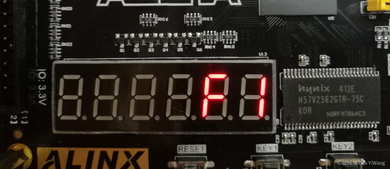
endendmodule7 实验结果
下载实验程序后,可以看到数码管显示一个数字,这个数字是存储在 sd 卡中第一扇区的第一
个数据,数据是随机的,这个时候按键 KEY1 按下,数字加一,并写入了 sd 卡,再次下载程序,
可以看到直接显示更新后的数据。

8 参考资料
【1】百度百科:EEPROM
【2】百度百科:NOR FLASH
【3】百度百科:NAND FLASH
【4】黑金社区
【5】基于FPGA的SD卡的数据读写实现(SD NAND FLASH)
需要工程文件(Quartus工程文件)的小伙伴也可以在公众号“Alex的书桌与实验室”回复“1SD”获取下载链接~
这就是本期的全部内容啦,如果你喜欢我的文章,不要忘了点赞+收藏+关注,分享给身边的朋友哇~