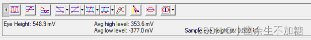
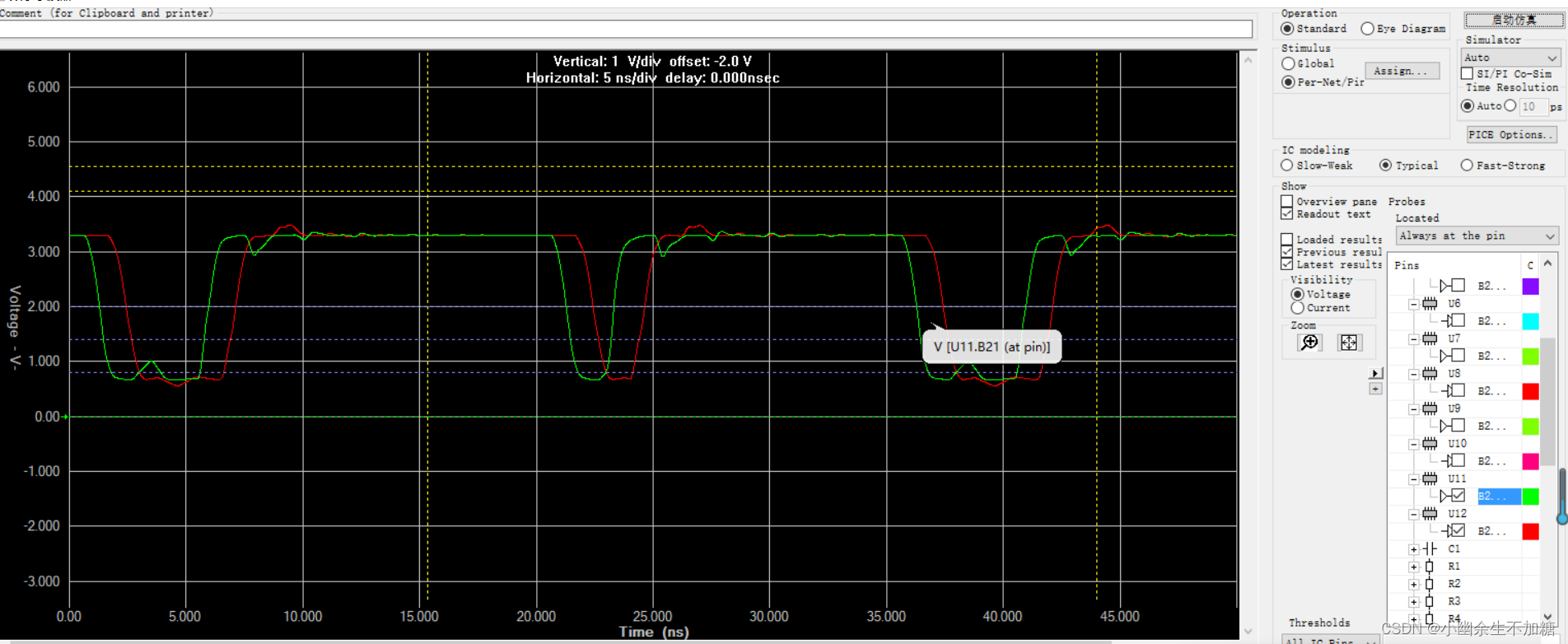
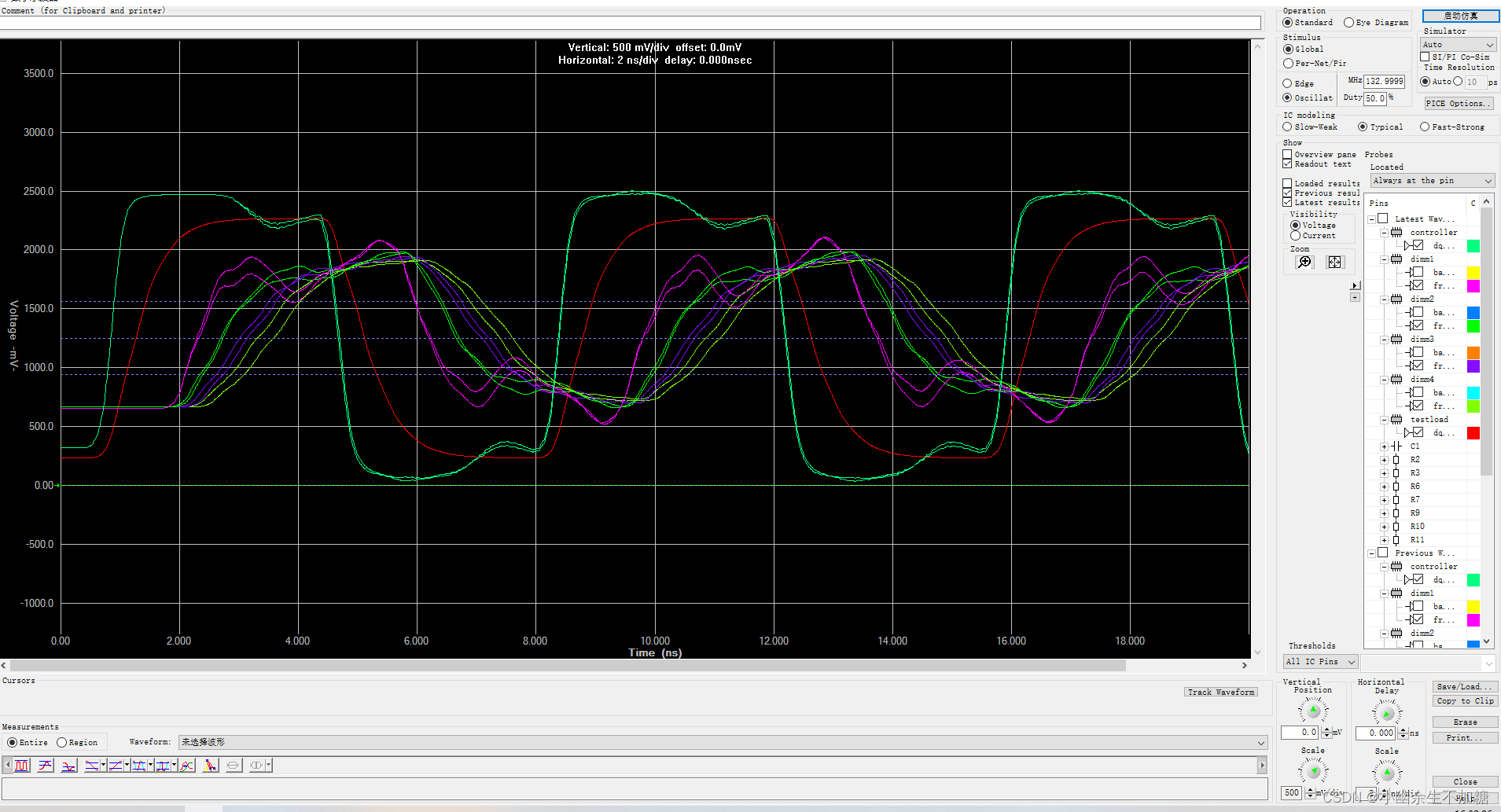
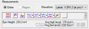
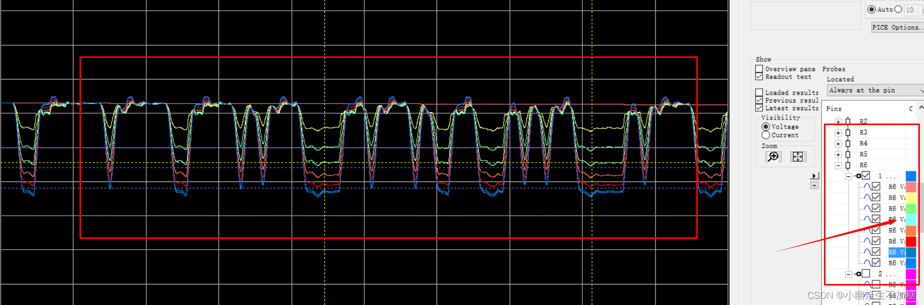
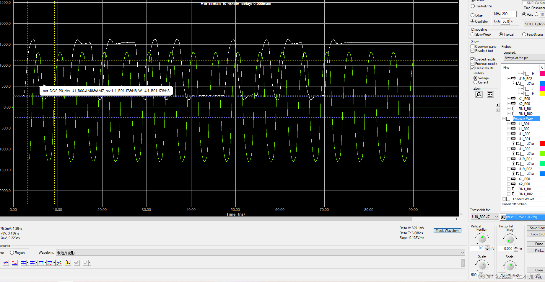
这是一篇基于Mentor公司 Hyperlynx VX.2.5 仿真软件针对Xilinx ZYNQ 的ZC702 PCB上DDR3内存布局布线的信号完整性仿真分析。层叠结构设置,关键信号的仿真分析,有助于我们了解基于 Hyperlynx 对 DDR3 进行信号完整性仿真的整个流程。
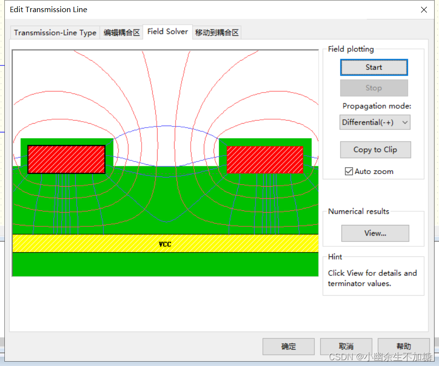
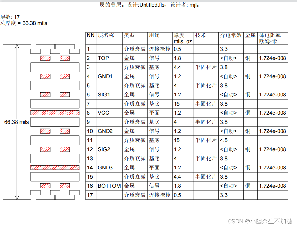
首先我们从实际出发,我们根据实际板厂的叠层结构阻抗计算,调整了原PCB的叠层结构。
首先打开Hyperlynx VX.2.5,导入brd文件。

After open a board, Verifying That the Software Recognizes Your Design Correctly.
1、Verifying That Power Supply and Signal Nets are Recognized Correctly 电源和信号网络
Ensure that the software recognizes the power supply nets in your design correctly. If it does not, specify them manually. Nets that are not recognized as power supply nets are recognized as signal nets.
The software automatically attempts to recognize power supply nets. The automatic
identification algorithm can miss power supply nets with arbitrary names or few capacitor connections, and short power supply nets that are connected to a voltage regulator module.
The software automatically recognizes a net as a power supply net if three or more capacitor are connected to it, or if it is connected to 100 or more vias. You can change these values in the Net handling area of the Preferences dialog box (Setup > Options > General > BoardSim tab).
Look for these indications that power supply nets are not recognized correctly:
- Undetected power supply nets can lead to some nets looking complicated and huge in the board viewer. This occurs because the software displays not only the chosen net, but also all non-power supply nets connected to the chosen net through passive components(e.g., resistors and capacitors). The connected nets are called associated nets.
- Simulation runs very slow, as the software attempts to simultaneously analyze huge sets of nets that are erroneously tied together.
编辑电源网络过程:
- Choose Setup > Power Supplies. The Edit Power Supply Nets dialog box opens.
- Ensure that all power supply (power and ground) nets in your design are checked in the list. If your design includes many obscurely-named power supply nets, use the Power Supply Nets Assistant to find other power supply nets that are connected to the main power supply nets by components. To use the assistant:
a. Select the main power supply nets in your design, then click Assist.
b. In the Power Supply Nets Assistant dialog box, select a power supply net. Connected components appear in a list to the right.
c. Select any non-terminating components from the Connected components list that are likely to connect to other power supply nets. For example, ferrite beads, inductors, bypass capacitors, and some resistors.
d. Select any connected power supply nets from the Connected nets list and click Add to power-supplies.
3. Ensure that the correct voltage is assigned to power supply nets in the “Edit supply voltages” list. To change the power supply voltage for specific nets, type a value in the Voltage column.
4. Ensure that any power supply nets connected to a plane layer (defined as type “plane” without any copper shapes) are listed in the “Assign supply nets to plane layers” list. To associate a plane layer with a supply net, next to each plane layer, click the supply net name and select the correct net from the list. This step is not required for most fully routed designs.
5. Click OK

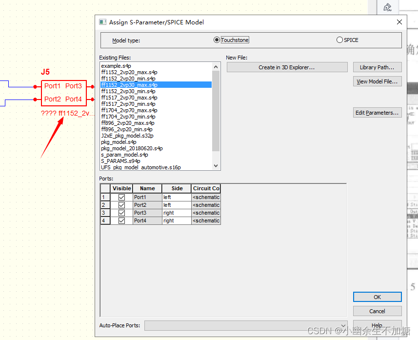
2、Verifying That Component Types are Recognized Correctly 器件模型
To ensure that the software recognizes components correctly, and your components appear in model assignment lists correctly, edit reference designator mappings.
The software recognizes a component as a resistor, inductor, IC, or other component type, by reading the prefix of the reference designator associated with the component.
Review these tips before proceeding:
- Unrecognized components are mapped as ICs by default.
- The software does not recognize diodes, transistors, relays, or crystals as specific
component types. Map these components as ICs. - To describe a discrete clamp diode or diode-terminating network, map diodes as ICs and assign an IBIS model that contains information describing the diode.
为了描述一个离散箝位二极管或二极管端接网络,将二极管映射为集成电路,并指定一个包含描述二极管信息的IBIS模型。
- If you choose the “Design independent” option, reference-designator mappings are
global and apply to all designs. If you choose the “Design-specific” option, reference designator mappings apply only to the current design. - If you make “Design-specific” changes to reference-designator mappings, you must reload the design for the changes to take effect.
- Mappings at the top of the list have highest priority. Mappings are sorted into groups based on the number of characters in the reference prefix and then alphabetically sorted within the groups.
Procedure
1. Choose Setup > Options > Reference Designator Mappings.
2. To review current mappings, scroll through the Mappings list.
3. If you have loaded a design, choose either to have your mapping apply to all designs
(“Design independent”) or apply only to the current design (“Design-specific”). If you
haven’t loaded a design, your mapping applies to all designs.
4. You can either create a new component type or change the mapping of an existing
component type:
- To create a new mapping, type the new reference designator (Ref.) prefix and choose the component type from the radio buttons.
- To change an existing mapping, select a component type from the Mappings list and then choose a new component type from the radio buttons.
5. Click Add/Apply.
6. Choose Models > Assign Models/Values by Reference Designator to open the Ref
File Editor. Scroll through the list of parts to ensure that all components are recognized
correctly

3、Verifying That Differential Pairs are Recognized Correctly 差分信号
Ensure that the software recognizes differentially paired nets correctly, so it can simulate them correctly. Create net name pairing rules to specify how the software automatically identifies paired nets when a board is loaded. You can also specify differential pairs manually for a design.
When you open a board design, the software reads differential pair identifying information from any assigned IBIS models, identifies nets connected by parallel terminators, and then reads the names of the remaining nets and attempts to recognize differentially paired nets based on the names of the nets.
Restrictions and Limitations 限制和局限
- Both nets in a differential pair must connect to at least one pair of pins on the same
reference designator. - Net naming rules do not apply to net pairs that are already identified by information in assigned IBIS models, or net pairs connected by parallel terminators. The net names in IBIS models must match the net names in your design to be recognized correctly.
Procedure
- With your board design open, select Setup > Differential Pairs. Check the list of differential pairs and verify that any differentially paired nets that you want to simulate are recognized.
- Set up differential pairing rules to enable the software to recognize differential pairs automatically when you load a board, or manually specify paired nets for your design.
| If you want to... | Do this... |
| Create a pairing rule that applies to all designs | 1. Under Differential pair net names, type characters |
| Manually specify paired nets for your
| 1. In the Nets list, select two nets and click the arrow button to add them to the list of paired nets on the right.
|
- Leave Rebuild differential pairs when loading unchecked if you want manually specified pairings to be saved when you save the session.
- Click OK.

4、Verifying the Stackup Definition 叠层结构
Verify that the stackup definition accurately represents your design.
Note
If you have a board design with multiple stackups, see Verifying the Stackup Definition for a Board Design With Multiple Stackups.
Prerequisites 先决条件
- Disable the Enable Multiple Stackups menu item (choose the menu item to deactivate its check mark)
Procedure
- Choose Setup > Stackup > Edit. The Stackup Editor opens.
- Verify the stackup definition, and make changes as needed. To change the stackup
definition, see “Defining the Basic Stackup”.

Verifying the Stackup Definition for a Board Design With Multiple Stackup
Verify that the stackup layer and stackup area definitions accurately represent your design.
Prerequisites
- You understand Board Designs With Multiple Stackups.
- The master stackup definition contains all the layers used by stackup areas in your
design. - Enable the Enable Multiple Stackups menu item (choose the menu item to activate its check mark).
Procedure
1. Choose Setup > Stackup > Stackup Manager. The Stackup Manager dialog box
opens.
2. Verify stackup definitions:
a. Select a stackup and click Edit. The Stackup Editor opens.
b. Verify that the stackup represents your design, and make changes as needed. See Defining the Basic Stackup.
c. In the Stackup Manager dialog box, verify that the spreadsheet contains a stackup
definition for each stackup area in your design, and add stackups as needed. See
Defining a Stackup for a Board Design With Multiple Stackups.
d. Repeat steps a - c for other stackups and boards (for a multiple-board design).
3. Verify that each area of your board design has the correct stackup assigned to it:
a. In the Stackup Manager dialog box, select a stackup and click Select Area. The
board viewer highlights the area(s) assigned to the stackup. To remove highlighting,
click Select Area again.
b. Make stackup area changes or additions as needed. See Defining a Stackup Area for
a Board Design With Multiple Stackups.
Note
The software automatically assigns the master stackup to areas of your board design without a stackup area assigned to them.