1、Single Choice: Given the following FIFO and rules, how deep does the FIFO need to be to prevent underflow or overflow?
RULES:
clk_A=25MHz;
clk_B=100MHz;
en_B is periodically asserted: period is 4us, dutycycle is 25%
Pick ONE option
A. 100 entries
B. 75 entries
C. FIFO will overflow anyway
D. 10 entries
解:B

2、Assuming a=1'b1; b=1'b0 what's the final values of a and b?
| ① always@(posedge clk) begin a=b; b=a; end | ② always@(posedge clk) a=b; always@(posedge clk) b=a; | ③ always@(posedge clk) begin a<=b; b<=a; end | ④ always@(posedge clk) a<=b; always@(posedge clk) b<=a; |
| a= ? b= ? | a= ? b= ? | a= ? b= ? | a= ? b= ? |
解:
1、a=0 b=0
2、? 我猜每次仿真结果都不一样,always执行顺序不同
3、a= 0 b=1
4、A=0 B=1
【Verilog HDL】赋值语句之阻塞赋值方式与非阻塞赋值方式_李锐博恩的博客-CSDN博客_verilog 阻塞赋值
3、What are commonly used techniques to reduce dynamic power in low power design?
Pick ONE OR MORE options
A. Bus signal encoding, bus decoding (5 points)
B. Clock gating
C. Power gating
D. Dynamic voltage and frequency scaling(DVFS)
E. Body biasing
解:查了一下感觉选abcde
BCD我知道
A 总线编解码,大概就是通过编码来减少信号翻转率来降低功耗
Bus encoding/decoding apparatus and method - 百度学术https://xueshu.baidu.com/usercenter/paper/show?paperid=1r4y0rv0mr4f0g804v2k0tk0yk051550
A bus encoding/decoding apparatus and method for a low power digital signal processor (DSP), which uses a narrow data bus, is provided. The apparatus for encoding n bits of data of a data bus, includes a conditional inverting unit for inverting each of (n1) lower bits of n data when the most significant bit of the n bits of data is 1, a storage unit for storing the last n bits of data which is output to the bus, and a first exclusive OR operating unit for performing a bitwise exclusive OR operation on the lower (n1) bits or data, which has been inverted by the conditional inverting unit, and the lower (n1) bits of the n data, which has been stored in the storage unit, wherein the most significant bit of the n bits of data and (n1) bits of data, which is obtained as the result of the bitwise exclusive OR operation performed by the first exclusive OR operating unit, are output. Accordingly, interface problems with a core and overhead for an additional circuit can be reduced by removing the additional circuit for determining whether to invert data and an extra line, which are used in the conventional BI and BITS coding methods, thereby decreasing the power consumption and the area of a chip.
D基体偏压
重新定义低功耗、小尺寸FPGA-EDN 电子技术设计物联网AI、嵌入式视觉、硬件安全、5G通信、工业和汽车自动化等新兴应用正在重新定义开发人员设计网络边缘产品的硬件要求。
https://www.ednchina.com/news/202005261413.html
FD-SOI工艺让莱迪思的工程师能够开发全新电路设计,充分发挥该工艺的固有优势。其优势之一就是FD-SOI支持可编程基体偏压(body bias),这是一种位于晶体管基体上的块电阻,能让开发人员在晶体管运行期间进行动态调节。莱迪思的研发团队发明的可编程基体偏压,能够根据设计的功耗和散热管理需要,让器件以高性能模式或低功耗模式运行。只需通过软件开关即可控制运行模式。开发人员通过对基体偏压进行编程实现高性能或低功耗之间的切换,可以优化 FPGA 的功耗/性能,更好地满足应用的功耗和散热管理需求。这不仅有助于降低电池供电的网络边缘设备的功耗,还能降低工业和数据中心等应用的电力成本。根据莱迪思估算,基于Nexus平台的FPGA的功耗将比同类竞品最多减少75%。
Bus encoding/decoding apparatus and method - 百度学术![]() https://xueshu.baidu.com/usercenter/paper/show?paperid=1r4y0rv0mr4f0g804v2k0tk0yk051550
https://xueshu.baidu.com/usercenter/paper/show?paperid=1r4y0rv0mr4f0g804v2k0tk0yk051550
4、There is a triangle andon it there are 3 ants, one on each corner and they are free to move alongsides of triangle. What is probability that they will collide?
Pick ONE option
A. 1/8
B. 1/4
C. 3/8
D. 3/4
不想做这种东西
5、Complete the blanks inthe following question with the appropriate answer.
Select the appropriate asynchronous technical terms tothe corresponding sequence number.
CDC Check Clock Domain Crossing Check.
MTBF Check Mean Time Between Failure Check.
Glitch Check Combinational logic will cause glitch violationin sync path, it can be covered by STA Make sure no combinational logic beforea synchronizer.
Reconvergence Check: Signals synced by a groupsynchronizers can't merged into combinational logic immediately.
B2B Check: Two beat approach by flops are usually usedto handle asynchronous paths. But there is no quantized parameters to calculateMTBF by this approach.
Async Timing Check Async path timing status is notcovered by STA We use scripts to capture related timing to check these paths.
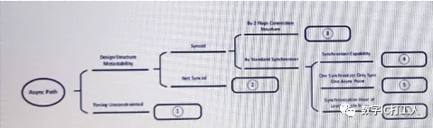
解:这图好糊 、
6、Complete the blanks inthe following question with the appropriate answer.
There is a FIFO, at the input side, there will be atmost 80 valid input out of 100 cycles; at the output side there will be at least 8 available slots out of 10 cycles, please specify what is the minimized FIFO depth for this case.

Depth=_____106____
160*(80/100)- 160*(10/100)*(8/10)=128-12.8=106
有空画一遍

7、The following schematicshows datapath operators going into a register. From power perspective, figureout the inefficient part and draw a new schematic with your fix.
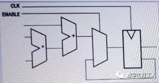
这D触发器的q和q‘没写,先当q‘做吧

时钟门控终极指南 - 知乎![]() https://zhuanlan.zhihu.com/p/390828391
https://zhuanlan.zhihu.com/p/390828391
8 、There is a counter can down count from 60 to 0. When the count reaches 0, the count will alarm. There are 4 buttonson the counter (they can all be treated as pulse signals). Users are allowed topress merely 1 button each time. When the counter is alarming, press ‘add’ or ‘clear’buttons will stop alarming.
Button 'start':press 'start' button,the counter will start downcount to 0.
Button 'clear':press 'clear' button,the counter will be back to 60 and stop counting.
Button 'hold':press 'hold' button, thecounter will stop countering, until press 'start' or 'clear' button ('add'button doesn't work when hold).
Button 'add'
press 'add' button, the counter will add 10 (Forexample, when the counter is 20, press 'add' then the counter will go back to 30. When the counter is 54, press 'add' then the counter will go back to 60.)
Please draw the finite state machine diagram
Please describe the counter in verilog using the ftmyou design in question 1(clock signal: clk, reset signal: rst_n) Output alarm(when the counter is arming, alarm=1). Output [5:0] counter_num from (60 to 0)
Please use below module definition to start with:
module downcounter(input clk,input rst_n,//funcbuttonsinput start,input clear,input hold,input add,output alarm,output[5:0] counter_num);endmodule
ADD状态转移不知道画的对不对
9、Suppose there is a logfile
The file's content is like: <MESSAGE LEVEL>_<MESSAGE_TYPE>_<MESSAGE_ CONTENT>
<MESSAGE_ LEVEL> should be "ERROR" or"WARNING" or "INFO"
<MESSAGE_TYPE> should be "TYPE" plusan integer number.
Please write a function named as printErrors to parsethe log, filter out required information and print some messages. Given astring logPath representing the log file path.
The requirements are:
a. The output messages should be ERROR level and theirMESSAGE_CONTENT should contain “NVIDIA_SOC”
b. Sorted the output order by MODULE_TYPE number
c. Use any script language you like.
###
Example 1:
log file.
ERROR_TYPE1_NVIDIA
INFO_TYPE1_NVIDIA SOC
ERROR_ TYPE4_THIS_IS_NVIDIA_SOC
WARNING_TYPE2_SOC
ERROR_TYPE1_SOC
ERROR_TYPE1_NVIDIA_SOC_TEAM
ERROR_TYPE4_NVIDIA_SOC
ERROR_TYPE12_NVIDIA_SOC
Example 2:
log file:
ERROR_TYPE1_NVIDIA
ERROR_TYPE12_NVIDIA_SOC
ERROR_TYPE1_Nvidia_soc
INFO_TYPE2_NVIDIA_SOC TEAM
ERROR TYPE12 NVIDIA SOC
###
Please provide your answer in the following editor
学完tcl在写
10、Gate level logic netlist_ais optimized to netlist_b in back-end flow. And they are checked by formalcheck tool to prove whether they are functional equivalence. Please answer belowquestions.

1.What is the concept of combinational and sequential logic?Please classify A/B/C/D cells in below netlist_a schematic, which belong tocombinational logic and which belongs to sequential logic?
组合逻辑

时序逻辑

bcd组合逻辑,a时序逻辑
2. If the value vector 110 is applied to the leftthree flops D pin After 1 cycle what is the D pin value of the reg_d in netlist_a/netlist_b?


3. Please estimate if above netlists are functionequivalent or not according to the netlist schematics and explain why?
不等效吧
第一个化简得 :第一个看不清,到底是vdd还是gnd?
假设是vdd,结果是a+b^c
如果是gnd,结果是a+b'c
第二个化简得:a'+b^c
但不管是啥,a的路径都不等价吧
11、3-stages pipelinecircuit shown as below.
The clock period is 0.9
The clock uncertainty is 0.1
The cell delay for F1/F2/F3 from CP-> Q are 0.15
The library setup require time for F1/F2/F3 are 0.1
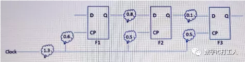
1. Please calculate the setup slack between F1 and F2

写错了 slack减反了,应该是-0.25ns
2. Please describe what's clock skew and suggest how to fix the setup violation between F1 and F2 with clock skew

换一个速度快的寄存器,降低温度,降低时钟频率,加流水线,缩短关键路径,在f2时钟路径上加buffer

3. Please recalculate the slack between F2 and F3 after the setup violation between F1 and F2 are fixed to 0
【STA专题四】时序约束 - 知乎
setup slack = 0.9-0.15-0.1 = 0.75
12、Please use NAND2 gates to create new logic signal as below: (Use as less gates as possible) New_ logic= ECO_SELECT? Original_logic & mask: original logic;

=[o’+(m+E')']’

13、Design a sequence(10100) detector. The logic with single bit input and single bit output. When detectinginput bit with the sequence of 10100 output pulse with one cycle of 1'b1,otherwise output keeps 1'b0. (No need to write RTL code, just provide aschematic diagram or a state machine flow chart.)

输出补一下斜杠,我忘写了
14、Design a block (WriteVerilog code) with below requirement:
Block interfaces: data_in[31:0], data_ in_valid, data_out[31:0],data_out_valid, clock, reset_;
Function: Input package of data_in and output packageof data_out both include 4 bytes of data, and we expect that data_out containsthe 4 bytes data from the same position but in different input cycle. (i.e.output cycle 0 contains the lowest bytes from input cycle 0 to 3; output cycle1 contains to second lowest bytes from input cycle 0 to 3; output cycle 2contains second highest bytes from input cycle 0 to 3; output cycle 3 containshighest bytes from input cycle 0 to 3; output cycle 4 contains lowest bytesfrom input cycle 4 to8...)
Timing requirement: data_out and data_out_valid need direct flop-driven.

【旧文】面试手撕代码真题详解-窄传输【开卷】海思面试手撕代码真题详解-窄传输https://mp.weixin.qq.com/s/cR7cgt5mfWtsCyWEPvyHrg有空写
FPGA/IC笔试——杂七杂八 - 一曲挽歌 - 博客园
2022英伟达(NVIDA)实习生笔试(ASIC PD岗位)_桐桐花的博客-CSDN博客_英伟达笔试