上篇文章主要讲了一些关于AXI的知识,有了这些理论,让我们进行一些简单的实验测试,加深对AXI协议的理解。本次实验使用的平台是VIVADO2019.1。
1. 首先创建一个工程,名称和路径自己决定。
2.然后按照图中所示,点击新建和打包一个新IP核。

3.点击NEXT
4.选择一个带AXI4接口的IP核,然后点击NEXT
5.记得修改名称,不然后边不好修改,路径可以直接放在工程根目录下
6.名称我们进行修改,然后选用FULL接口的AXI,选择IP核为主机,数据位宽选32bits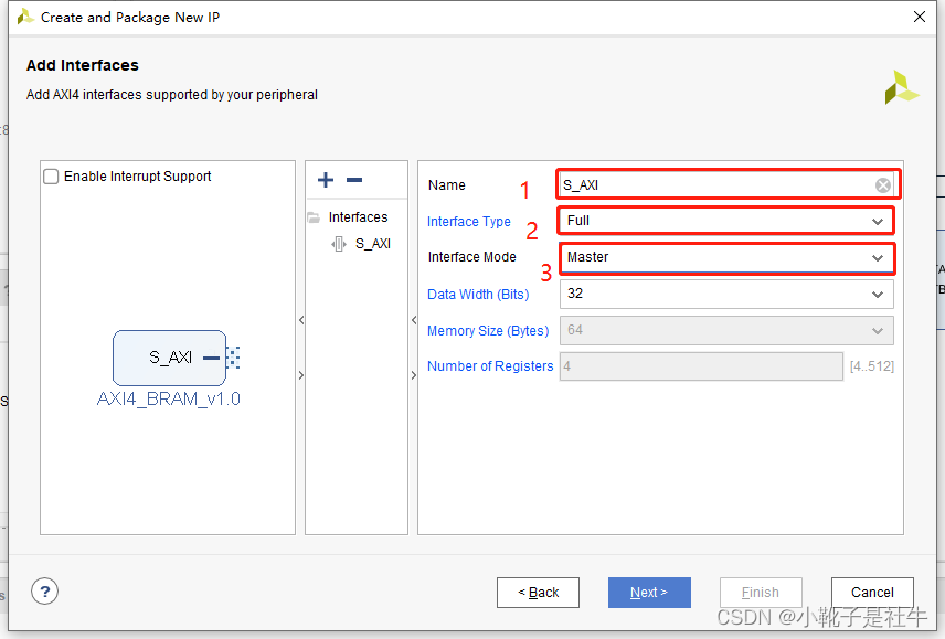
7.我们选择编辑此IP,我们便成功调用IP
8.IP设置完成后,我们可以看到里边的.v代码,主要就是一个测试模块,它实现的功能就是利用AXI4接口向外发送1024个数据,然后再将数据读回,通过对比来验证AXI4这个IP核的功能。我对生成的代码做了一些注释,大家可以对照理解,代码不需要动,可以直接使用。
`timescale 1 ns / 1 psmodule AXI4_v1_0_AXI_MASTER #(// Users to add parameters here// User parameters ends// Do not modify the parameters beyond this line// Base address of targeted slave               基地址parameter  C_M_TARGET_SLAVE_BASE_ADDR	= 32'h40000000,// Burst Length. Supports 1, 2, 4, 8, 16, 32, 64, 128, 256 burst lengths   突发长度parameter integer C_M_AXI_BURST_LEN	= 16,// Thread ID Width             写ID宽度parameter integer C_M_AXI_ID_WIDTH	= 1,// Width of Address Bus           写地址宽度parameter integer C_M_AXI_ADDR_WIDTH	= 32,// Width of Data Bus              写数据宽度parameter integer C_M_AXI_DATA_WIDTH	= 32,// Width of User Write Address Busparameter integer C_M_AXI_AWUSER_WIDTH	= 0,// Width of User Read Address Busparameter integer C_M_AXI_ARUSER_WIDTH	= 0,// Width of User Write Data Busparameter integer C_M_AXI_WUSER_WIDTH	= 0,// Width of User Read Data Busparameter integer C_M_AXI_RUSER_WIDTH	= 0,// Width of User Response Busparameter integer C_M_AXI_BUSER_WIDTH	= 0)(// Users to add ports here// User ports ends// Do not modify the ports beyond this line
//用户IO// Initiate AXI transactions 写开始信号input wire  INIT_AXI_TXN,// Asserts when transaction is complete写完成信号output wire  TXN_DONE,     // Asserts when ERROR is detected 数据检测信号output reg  ERROR,// Global Clock Signal. 全剧时钟input wire  M_AXI_ACLK,// Global Reset Singal. This Signal is Active Low  全局复位信号input wire  M_AXI_ARESETN,// Master Interface Write Address ID      写地址IDoutput wire [C_M_AXI_ID_WIDTH-1 : 0] M_AXI_AWID,// Master Interface Write Address        写地址output wire [C_M_AXI_ADDR_WIDTH-1 : 0] M_AXI_AWADDR,// Burst length. The burst length gives the exact number of transfers in a burstoutput wire [7 : 0] M_AXI_AWLEN,   //写长度// Burst size. This signal indicates the size of each transfer in the burstoutput wire [2 : 0] M_AXI_AWSIZE,  //写宽度// Burst type. The burst type and the size information, // determine how the address for each transfer within the burst is calculated.output wire [1 : 0] M_AXI_AWBURST, //写类型// Lock type. Provides additional information about the// atomic characteristics of the transfer.output wire  M_AXI_AWLOCK,  //独占传输类型// Memory type. This signal indicates how transactions// are required to progress through a system.output wire [3 : 0] M_AXI_AWCACHE,  //存储类型,指明是否缓存// Protection type. This signal indicates the privilege// and security level of the transaction, and whether// the transaction is a data access or an instruction access.output wire [2 : 0] M_AXI_AWPROT,  //安全保护// Quality of Service, QoS identifier sent for each write transaction.output wire [3 : 0] M_AXI_AWQOS,  //服务质量QOS// Optional User-defined signal in the write address channel. 用户自定义output wire [C_M_AXI_AWUSER_WIDTH-1 : 0] M_AXI_AWUSER,// Write address valid. This signal indicates that// the channel is signaling valid write address and control information.output wire  M_AXI_AWVALID, // 写地址发送有效,主机发给从机// Write address ready. This signal indicates that// the slave is ready to accept an address and associated control signalsinput wire  M_AXI_AWREADY,  //写地址接收有效,从机发给主机// Master Interface Write Data. 写数据 32位output wire [C_M_AXI_DATA_WIDTH-1 : 0] M_AXI_WDATA,// Write strobes. This signal indicates which byte// lanes hold valid data. There is one write strobe// bit for each eight bits of the write data bus.   频闪信号32/8 = 4位output wire [C_M_AXI_DATA_WIDTH/8-1 : 0] M_AXI_WSTRB,// Write last. This signal indicates the last transfer in a write burst.output wire  M_AXI_WLAST, //写数据最后一位// Optional User-defined signal in the write data channel.output wire [C_M_AXI_WUSER_WIDTH-1 : 0] M_AXI_WUSER, //用户自定义// Write valid. This signal indicates that valid write// data and strobes are available  写数据发送有效,主到从output wire  M_AXI_WVALID,// Write ready. This signal indicates that the slave// can accept the write data. //写数据接收有效,从到主input wire  M_AXI_WREADY,// Master Interface Write Response. 写响应IDinput wire [C_M_AXI_ID_WIDTH-1 : 0] M_AXI_BID,// Write response. This signal indicates the status of the write transaction.input wire [1 : 0] M_AXI_BRESP, //写响应信号// Optional User-defined signal in the write response channelinput wire [C_M_AXI_BUSER_WIDTH-1 : 0] M_AXI_BUSER, // 用户自定义// Write response valid. This signal indicates that the// channel is signaling a valid write response.input wire  M_AXI_BVALID,  //写响应信号发送有效,从到主// Response ready. This signal indicates that the master// can accept a write response.output wire  M_AXI_BREADY, //写响应信号接收有效,主到从// Master Interface Read Address.读地址IDoutput wire [C_M_AXI_ID_WIDTH-1 : 0] M_AXI_ARID,// Read address. This signal indicates the initial// address of a read burst transaction. 读地址output wire [C_M_AXI_ADDR_WIDTH-1 : 0] M_AXI_ARADDR,// Burst length. The burst length gives the exact number of transfers in a burstoutput wire [7 : 0] M_AXI_ARLEN,  //读突发长度// Burst size. This signal indicates the size of each transfer in the burstoutput wire [2 : 0] M_AXI_ARSIZE, //读突发大小// Burst type. The burst type and the size information, // determine how the address for each transfer within the burst is calculated.output wire [1 : 0] M_AXI_ARBURST, //读突发类型// Lock type. Provides additional information about the// atomic characteristics of the transfer.output wire  M_AXI_ARLOCK,  //总线锁信号// Memory type. This signal indicates how transactions// are required to progress through a system.output wire [3 : 0] M_AXI_ARCACHE, //Cache类型,是否缓存// Protection type. This signal indicates the privilege// and security level of the transaction, and whether// the transaction is a data access or an instruction access.output wire [2 : 0] M_AXI_ARPROT, //保护类型// Quality of Service, QoS identifier sent for each read transactionoutput wire [3 : 0] M_AXI_ARQOS, //质量服务// Optional User-defined signal in the read address channel.output wire [C_M_AXI_ARUSER_WIDTH-1 : 0] M_AXI_ARUSER,// Write address valid. This signal indicates that// the channel is signaling valid read address and control informationoutput wire  M_AXI_ARVALID, //读地址发送有效,主到从// Read address ready. This signal indicates that// the slave is ready to accept an address and associated control signalsinput wire  M_AXI_ARREADY, //读地址接收有效,从到主// Read ID tag. This signal is the identification tag// for the read data group of signals generated by the slave.input wire [C_M_AXI_ID_WIDTH-1 : 0] M_AXI_RID, //读数据ID// Master Read Data                  读数据input wire [C_M_AXI_DATA_WIDTH-1 : 0] M_AXI_RDATA, // Read response. This signal indicates the status of the read transferinput wire [1 : 0] M_AXI_RRESP,   //读响应信号// Read last. This signal indicates the last transfer in a read burstinput wire  M_AXI_RLAST,        //突发读传输的最后一个数据// Optional User-defined signal in the read address channel.input wire [C_M_AXI_RUSER_WIDTH-1 : 0] M_AXI_RUSER, //用户自定义信号// Read valid. This signal indicates that the channel// is signaling the required read data.input wire  M_AXI_RVALID, //读数据发送有效,从到主// Read ready. This signal indicates that the master can// accept the read data and response information.output wire  M_AXI_RREADY   //读数据接收有效。主到从);// function called clogb2 that returns an integer which has the//value of the ceiling of the log base 2// function called clogb2 that returns an integer which has the // value of the ceiling of the log base 2.                      function integer clogb2 (input integer bit_depth);         //计算信号的位宽     begin                                                           for(clogb2=0; bit_depth>0; clogb2=clogb2+1)                   bit_depth = bit_depth >> 1;                                 end                                                           endfunction                                                     // C_TRANSACTIONS_NUM is the width of the index counter for // number of write or read transaction.(4)                  C_TRANSACTIONS_NUM指读/写标识计数器的位宽localparam integer C_TRANSACTIONS_NUM = clogb2(C_M_AXI_BURST_LEN-1);// Burst length for transactions, in C_M_AXI_DATA_WIDTHs.// Non-2^n lengths will eventually cause bursts across 4K address boundaries.localparam integer C_MASTER_LENGTH	= 12;// total number of burst transfers is master length divided by burst length and burst sizelocalparam integer C_NO_BURSTS_REQ = C_MASTER_LENGTH-clogb2((C_M_AXI_BURST_LEN*C_M_AXI_DATA_WIDTH/8)-1);//12-6 = 6// Example State machine to initialize counter, initialize write transactions, // initialize read transactions and comparison of read data with the // written data words.parameter [1:0] IDLE = 2'b00, // This state initiates AXI4Lite transaction // after the state machine changes state to INIT_WRITE // when there is 0 to 1 transition on INIT_AXI_TXN 上升沿INIT_WRITE   = 2'b01, // This state initializes write transaction,// once writes are done, the state machine // changes state to INIT_READ INIT_READ = 2'b10, // This state initializes read transaction// once reads are done, the state machine // changes state to INIT_COMPARE INIT_COMPARE = 2'b11; // This state issues the status of comparison // of the written data with the read data	reg [1:0] mst_exec_state;// AXI4LITE signals//AXI4 internal temp signalsreg [C_M_AXI_ADDR_WIDTH-1 : 0] 	axi_awaddr; //32位写地址reg  	axi_awvalid;reg [C_M_AXI_DATA_WIDTH-1 : 0] 	axi_wdata;  //32位写数据reg  	axi_wlast;reg  	axi_wvalid;reg  	axi_bready;reg [C_M_AXI_ADDR_WIDTH-1 : 0] 	axi_araddr;  //32位读地址reg  	axi_arvalid;reg  	axi_rready;//write beat count in a burst 写计数5位reg [C_TRANSACTIONS_NUM : 0] 	write_index;//read beat count in a burst  读计数5位reg [C_TRANSACTIONS_NUM : 0] 	read_index;//size of C_M_AXI_BURST_LEN length burst in bytes 7位wire [C_TRANSACTIONS_NUM+2 : 0] 	burst_size_bytes;//The burst counters are used to track the number of burst transfers of C_M_AXI_BURST_LEN burst length needed to transfer 2^C_MASTER_LENGTH bytes of data.reg [C_NO_BURSTS_REQ : 0] 	write_burst_counter; //7位reg [C_NO_BURSTS_REQ : 0] 	read_burst_counter;  //7位reg  	start_single_burst_write;reg  	start_single_burst_read;reg  	writes_done;reg  	reads_done;reg  	error_reg;reg  	compare_done;reg  	read_mismatch;reg  	burst_write_active;reg  	burst_read_active;reg [C_M_AXI_DATA_WIDTH-1 : 0] 	expected_rdata;//Interface response error flagswire  	write_resp_error;wire  	read_resp_error;wire  	wnext;wire  	rnext;reg  	init_txn_ff;reg  	init_txn_ff2;reg  	init_txn_edge;wire  	init_txn_pulse;// I/O Connections assignmentswire douta;wire ena;//I/O Connections. Write Address (AW)assign M_AXI_AWID	= 'b0;//The AXI address is a concatenation of the target base address + active offset rangeassign M_AXI_AWADDR	= C_M_TARGET_SLAVE_BASE_ADDR + axi_awaddr;//Burst LENgth is number of transaction beats, minus 1assign M_AXI_AWLEN	= C_M_AXI_BURST_LEN - 1;//Size should be C_M_AXI_DATA_WIDTH, in 2^SIZE bytes, otherwise narrow bursts are usedassign M_AXI_AWSIZE	= clogb2((C_M_AXI_DATA_WIDTH/8)-1);//2'b10; 4BYTE//INCR burst type is usually used, except for keyhole burstsassign M_AXI_AWBURST	= 2'b01;  //INCR自增类型assign M_AXI_AWLOCK	= 1'b0;//Update value to 4'b0011 if coherent accesses to be used via the Zynq ACP port. Not Allocated, Modifiable, not Bufferable. Not Bufferable since this example is meant to test memory, not intermediate cache. assign M_AXI_AWCACHE	= 4'b0010;assign M_AXI_AWPROT	= 3'h0;assign M_AXI_AWQOS	= 4'h0;assign M_AXI_AWUSER	= 'b1;assign M_AXI_AWVALID	= axi_awvalid;//Write Data(W)assign M_AXI_WDATA	= douta;//All bursts are complete and aligned in this exampleassign M_AXI_WSTRB	= {(C_M_AXI_DATA_WIDTH/8){1'b1}};//4'B1111;assign M_AXI_WLAST	= axi_wlast;assign M_AXI_WUSER	= 'b0;assign M_AXI_WVALID	= axi_wvalid;//Write Response (B)assign M_AXI_BREADY	= axi_bready;//Read Address (AR)assign M_AXI_ARID	= 'b0;assign M_AXI_ARADDR	= C_M_TARGET_SLAVE_BASE_ADDR + axi_araddr;//Burst LENgth is number of transaction beats, minus 1assign M_AXI_ARLEN	= C_M_AXI_BURST_LEN - 1;//Size should be C_M_AXI_DATA_WIDTH, in 2^n bytes, otherwise narrow bursts are usedassign M_AXI_ARSIZE	= clogb2((C_M_AXI_DATA_WIDTH/8)-1);//INCR burst type is usually used, except for keyhole burstsassign M_AXI_ARBURST	= 2'b01;assign M_AXI_ARLOCK	= 1'b0;//Update value to 4'b0011 if coherent accesses to be used via the Zynq ACP port. Not Allocated, Modifiable, not Bufferable. Not Bufferable since this example is meant to test memory, not intermediate cache. assign M_AXI_ARCACHE	= 4'b0010;assign M_AXI_ARPROT	= 3'h0;assign M_AXI_ARQOS	= 4'h0;assign M_AXI_ARUSER	= 'b1;assign M_AXI_ARVALID	= axi_arvalid;//Read and Read Response (R)assign M_AXI_RREADY	= axi_rready;//Example design I/Oassign TXN_DONE	= compare_done;//Burst size in bytesassign burst_size_bytes	= C_M_AXI_BURST_LEN * C_M_AXI_DATA_WIDTH/8;//16*32/8 = 64assign init_txn_pulse	= (!init_txn_ff2) && init_txn_ff;//上升沿//Generate a pulse to initiate AXI transaction.always @(posedge M_AXI_ACLK)    //对输入按键信号打两拍,消除亚稳态begin                                                                        // Initiates AXI transaction delay    if (M_AXI_ARESETN == 0 )                                                   begin                                                                    init_txn_ff <= 1'b0;                                                   init_txn_ff2 <= 1'b0;                                                   end                                                                               else                                                                       begin  init_txn_ff <= INIT_AXI_TXN;init_txn_ff2 <= init_txn_ff;                                                                 end                                                                      end     //--------------------//Write Address Channel 写地址通道//--------------------// The purpose of the write address channel is to request the address and  写地址通道是传输整个传输过程中的首地址和控制信号// command information for the entire transaction.  It is a single beat    只传输一次// of information.// The AXI4 Write address channel in this example will continue to initiate// write commands as fast as it is allowed by the slave/interconnect.// The address will be incremented on each accepted address transaction,// by burst_size_byte to point to the next address. always @(posedge M_AXI_ACLK)                                   begin                                                                if (M_AXI_ARESETN == 0 || init_txn_pulse == 1'b1 )                                           begin                                                            axi_awvalid <= 1'b0;                                           end                                                              // If previously not valid , start next transaction                else if (~axi_awvalid && start_single_burst_write)                 begin                                                            axi_awvalid <= 1'b1;                                           end                                                              /* Once asserted, VALIDs cannot be deasserted, so axi_awvalid      must wait until transaction is accepted */                         else if (M_AXI_AWREADY && axi_awvalid)                             begin                                                            axi_awvalid <= 1'b0;                                           end                                                              else                                                               axi_awvalid <= axi_awvalid;                                      end                                                                // Next address after AWREADY indicates previous address acceptance    always @(posedge M_AXI_ACLK)                                         begin                                                                if (M_AXI_ARESETN == 0 || init_txn_pulse == 1'b1)                                            begin                                                            axi_awaddr <= 'b0;                                             end                                                              else if (M_AXI_AWREADY && axi_awvalid)                             begin                                                            axi_awaddr <= axi_awaddr + burst_size_bytes;        //突发长度为16,突发大小为4个字节,16*4=64           end                                                              else                                                               axi_awaddr <= axi_awaddr;                                        end                                                                //--------------------//Write Data Channel    写数据通道//--------------------//The write data will continually try to push write data across the interface.//The amount of data accepted will depend on the AXI slave and the AXI//Interconnect settings, such as if there are FIFOs enabled in interconnect.//Note that there is no explicit timing relationship to the write address channel.//The write channel has its own throttling flag, separate from the AW channel.//Synchronization between the channels must be determined by the user.//The simpliest but lowest performance would be to only issue one address write//and write data burst at a time.//In this example they are kept in sync by using the same address increment//and burst sizes. Then the AW and W channels have their transactions measured//with threshold counters as part of the user logic, to make sure neither //channel gets too far ahead of each other.//Forward movement occurs when the write channel is valid and readyassign wnext = M_AXI_WREADY & axi_wvalid;                            //wnext表示握手成功       // WVALID logic, similar to the axi_awvalid always block above                      always @(posedge M_AXI_ACLK)                                                      begin                                                                             if (M_AXI_ARESETN == 0 || init_txn_pulse == 1'b1 )                                                        begin                                                                         axi_wvalid <= 1'b0;                                                         end                                                                           // If previously not valid, start next transaction                              else if (~axi_wvalid && start_single_burst_write)                               begin                                                                         axi_wvalid <= 1'b1;                                                         end                                                                           /* If WREADY and too many writes, throttle WVALID                               Once asserted, VALIDs cannot be deasserted, so WVALID                           must wait until burst is complete with WLAST */                                 else if (wnext && axi_wlast)                                                    axi_wvalid <= 1'b0;                                                           else                                                                            axi_wvalid <= axi_wvalid;                                                     end
9.然后大家在Block Design中添加刚刚生成的这个IP核,再添加一个DRAM,然后对模块进行连接。BRAM我的配置如下所示:


然后其他的不用修改,直接添加,添加完成后对模块进行连接,使用一个控制模块将他们连起来。连接完成后如图所示: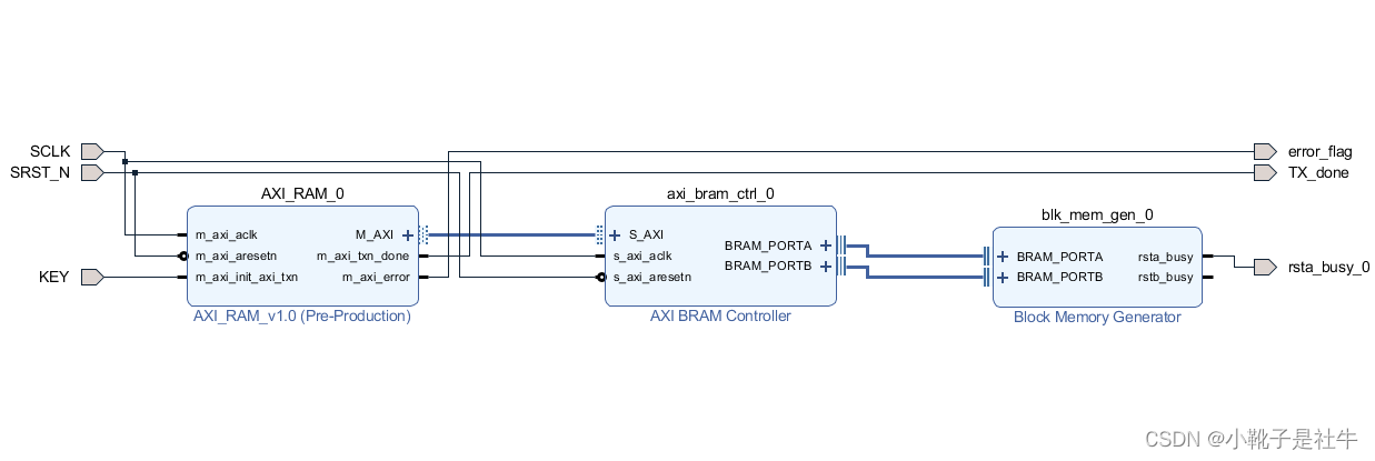
10.在完成上述工作后,我们便将AXI的IP核与BRAM连接起来了,通过AXI接口给BRAM发送数据,然后再将数据读出来,通过验证输出结果。TX_DONE表示发送成功,若得到错误的结果,会将erro_flag拉高。我们将这个设计打包成.v文件,具体操作如下。

11.这样我们就得到了这个测试系统的顶层文件,然后我们对其编写测试激励,仿真验证。
module tb_design_1();reg KEY;reg SCLK;reg SRST_N;wire TX_done;wire error_flag;wire rsta_busy_0;design_1 design_1(.KEY(KEY),.SCLK(SCLK),.SRST_N(SRST_N),.TX_done(TX_done),.error_flag(error_flag),.rsta_busy_0(rsta_busy_0));always #10 SCLK = ~SCLK;initial beginKEY = 0; SCLK = 0; SRST_N = 0;#201;SRST_N = 1;#100;KEY = 1;#200;KEY = 0;#200000;$stop;endendmodule
12.如图所示,前半部分是写数据,后半部分是读数据,最后可以看到发送完成信号TX_DONE信号拉高,而erro_flag没有拉高,我们也可以观察数据得到这个结果是正确的。
13.这样我们便通过AXI4的IP核对BRAM读写验证了功能的正确性,大家有兴趣的话可以看一下正点原子ZYNQ系列的视频,讲了该IP核去读写PS端DDR3的实验。
后续我还会总结一些关于DDR3相关的知识以及通过MIG去控制DDR3,实现该AXI4 IP核对DDR3进行读写的实验。