在基于ARM的嵌入式应用系统中,存储系统通常是通过系统控制协处理器CP15完成的。CP15包含16个32位的寄存器,其编号为0~15。
访问CP15寄存器的指令
MCR ARM寄存器到协处理器寄存器的数据传送
MRC 协处理器寄存器到ARM寄存器的数据传送
MCR指令和MRC指令只能在处理器模式为系统模式时执行,在用户模式下执行MCR指令和MRC指令将会触发未定义指令的异常中断。
MCR指令
MCR指令将ARM处理器的寄存器中的数据传送到协处理器寄存器中。如果协处理器不能成功地执行该操作,将产生未定义的指令异常中断。
指令语法格式
MCR{<cond>} <p>,< opcode_1>,<Rd>,<CRn>,<CRm>{,<opcode_2>}
MCR{<cond>} p15,0,<Rd>,<CRn>,<CRm>{,<opcode_2>}
其中,<cond>为指令执行的条件码。当<cond>忽略时指令为无条件执行。
< opcode_1>为协处理器将执行的操作的操作码。对于CP15协处理器来说,< opcode_1>永远为0b000,当< opcode_1>不为0b000时,该指令操作结果不可预知。
<Rd>作为源寄存器的ARM寄存器,其值将被传送到协处理器寄存器中。
<CRn>作为目标寄存器的协处理器寄存器,其编号可能是C0,C1,…,C15。
<CRm>和<opcode_2>两者组合决定对协处理器寄存器进行所需要的操作,如果没有指定,则将为<CRm>为C0,opcode_2为0,否则可能导致不可预知的结果。
The CRm field and opcode_2 field are used to specify a particular action when addressing registers.The opcode_1, opcode_2 and CRm fields should be zero, except when the values specified are used to select the desired operations, in all instructions which access CP15. Using other values will result in unpredictable behavior. Attempting to read from a non-readable register, or writing to a non-writable register will cause unpredictable results.
使用示例
下面的指令从ARM寄存器R4中中将数据传送到协处理器CP15的寄存器C1中。其中R4为ARM寄存器,存放源操作数,C1、C0为协处理器寄存器,为目标寄存器,opcode_1为0,opcode_2为0。
MCR p15, 0, R4, C1, C0, 0
MRC指令
MRC指令将协处理器的寄存器中的数值传送到ARM处理器的寄存器中、如果协处理器不能成功地执行该操作,将产生未定义的指令异常中断。
指令语法格式
MRC{<cond>} <p>,< opcode_1>,<Rd>,<CRn>,<CRm>{,<opcode_2>}
MRC{<cond>} p15,0,<Rd>,<CRn>,<CRm>{,<opcode_2>}
参数用法同MCR指令
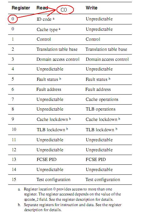
CP15中的寄存器介绍
| Register(寄存器) | Read | Write |
|
| C0 | ID Code (1) | Unpredictable |
|
| C0 | Catch type(1) | Unpredictable |
|
| C1 | Control | Control |
|
| C2 | Translation table base | Translation table base |
|
| C3 | Domain access control | Domain access control |
|
| C4 | Unpredictable | Unpredictable |
|
| C5 | Fault status(2) | Fault status (2) |
|
| C6 | Fault address | Fault address |
|
| C7 | Unpredictable | Cache operations |
|
| C8 | Unpredictable | TLB operations |
|
| C9 | Cache lockdown(2) | Cache lockdown (2) |
|
| C10 | TLB lock down(2) | TLB lock down(2) |
|
| C11 | Unpredictable | Unpredictable |
|
| C12 | Unpredictable | Unpredictable |
|
| C13 | Process ID | Process ID |
|
| C14 | Unpredictable | Unpredictable |
|
| C15 | Test configuration | Test configuration |
|
Notes:
1. Register location 0 provides access to more than one register. The register accessed depends upon values of the opcode_2 field. See the register description for details.
2. Separate register for instruction and data .See the register description for details.
寄存器0:ID Code Register
This is a read-only register which returns a 32-bit device ID code
这是一个只读寄存器,它存放微处理器的标识码。
The ID code register is accessed by reading CP15 register 0 with the opcode_2 field set to any value other than 1(the CRm field should be zero when reading). For example:
MRC p15, 0, Rd, C0, C0, 0
ID Code内容如下:
| Register bits | Function | Value |
| [31:24] | Implementor | 0x41(‘A’,表示Arm公司) |
| [23:20] | Specification revision | 0x1 |
| [19:16] | Architecture version(4T) | 0x2(ARM体系版本4T) |
| [15:4] | Part number | 0x920 |
| [3:0] | Layout revision | 0x0 |
寄存器0:Cache type register
This is a read-only register which contains information about the size and architecture of the caches, allowing operating systems to establish how to perform such operations as cache cleaning and lockdown.
这个只读寄存器包含了高速缓存的大小和类型。
The cache type register is accessed by reading CP15 register 0 with the opcode_2 field set to 1.for example:
MRC p15, 0, Rd, C0, C0, 1; returns cache details
The format of cache type register (寄存器的数据格式如下)
| Register bits | Function | Value |
| [31:29] | Reserved | 000 |
| [28:25] | Cache type (缓存类型) | 0110 |
| [24] | Harvard/Unified | 1(defines Harvard cache) |
| [23:21] | Reserved | 000 |
| [20:18] | Data Cache size(数据缓存大小) | 101(defines 16KB) |
| [17:15] | Data Cache associativity | 110(defines 64 way) |
| [14] | Reserved | 0 |
| [13:12] | Data Cache words per line | 10(defines 8 words per line) |
| [11:9] | Reserved | 000 |
| [ 8:6] | Instruction Cache size(指令缓存大小) | 101(defines 16KB) |
| [5:3] | Instruction Cache Associativity | 110(defines 64 way) |
| [2] | Reserved | 0 |
| [1:0] | Instruction Cache per line | 10(defines 8 words per line) |
寄存器1:Control register
对该寄存器读写指令如下:
MRC p15, 0, Rd, c1, c0, 0 ; read control register
MCR p15, 0, Rd, c1, c0, 0 ; write control register
该寄存器功能如下表
| Registe bits | Name | Function | Value |
| 31 | iA bit | Asynchronous clock select | 见时钟模式表 |
| 30 | nF bit | notFastBus select | 见 时钟模式表 |
| 29:15 | - | Reserved | Read = Unpredictable Write = should be zero |
| 14 | RR bit | Round robin replacement | 0 = Random replacement 1 = Round robin replacement |
| 13 | V bit | Base location of exception register(异常寄存器基地址) | 0 = Low address = 0x0000 0000 1 = High address = 0xFFFF 0000 |
| 12 | I bit | Instruction cache enable | 0 = Instruction cache disable 1 = Instruction cache enable |
| 11:10 | - | Reserved | Read = 00 Write = 00 |
| 9 | R bit | ROM protection | 见图1 |
| 8 | S bit | System protection | 见图1 |
| 7 | B bit | Big-endian/little-endian | 0 = Little-endian operation 1 = Big-endian operation |
| 6:3 | - | Reserved | Read = 1111 Write = 1111 |
| 2 | C bit | Data cache enable | 0 = data cache disable 1 = data cache enable |
| 1 | A bit | Alignment fault enable | Data address alignment fault checking (地址对齐检查) 0 = 禁用地址对齐检查功能 1 = 使能地址对齐检查功能 |
| 0 | M bit | MMU enable | 0 = MMU disable 1 = MMU enable |
时钟模式表
| Clocking mode(时钟模式) | iA | nF |
| Fastbus mode (快速总线模式) | 0 | 0 |
| Reserved | 1 | 0 |
| Synchronous (同步模式) | 0 | 1 |
| Asynchronous (异步模式) | 1 | 1 |

图1
寄存器2:Translation Table Base(TTB) Register
| Register bits | Function |
| 31:14 | Pointer to first level translation table base . Read /write |
| 13:0 | Reserved Read = Unpredictable Write = Should be zero |
访问C2寄存器指令如下:
MRC p15, 0, Rd, C2, C0, 0 ; Read TTB register
MCR p15, 0, Rd, C2, C0, 0 ; Write TTB register
该寄存器存放第一级转换表基地址。写入时,位[13:0]必须为0,读出时,位[13:0]的值不可预知。
寄存器3:Domain Access Control Register
寄存器3是可读写的域访问控制寄存器,分为16组,每组占用2个位

访问该寄存器的指令如下:
MRC p15, 0, Rd, C3, C0, 0 ; Read domain 15:0 access permissions
MCR p15, 0, Rd, C3, C0, 0 ; Read domain 15:0 access permissions
Interpreting Access Control Bits in Domain Access Control Register

寄存器4:保留
对该寄存器的读写会产生不可预料的结果。
寄存器5:Fault Status Register
寄存器6:Fault Address Register
寄存器7:Cache Operations
该寄存器是只写寄存器,用于管理指令缓存和数据缓存。
对该寄存器的写操作所实现的功能,是通过MCR指令中的opcode_2和CRm两者的组合来选择的,具体组合如下。

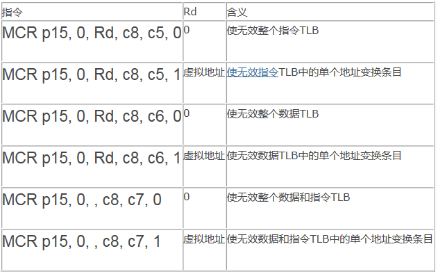
寄存器8:TLB Operations
Register 8 is a write-only register used to manage the translation lookaside buffer(TLBs),the instruction TLB and the data TLB.
Five TLB operations are defined and the function to be performed is selected by the opcode_2 and CRm fields in the MCR instruction used to write CP15 register 8.Writing other opcode_2 or CRm values id unpredictable. Reading from CP15 register 8 is unpredictable.
| Function | Data | instruction |
| Invalidate TLB(s) | SBZ | MCR p15,0,Rd,c8,c7,0 |
| Invalidate I TLB | SBZ | MCR p15,0,Rd,c8,c5,0 |
| Invalidate I TLB single entry (using MVA) | MVA format | MCR p15,0,Rd,c8,c5,1 |
| Invalidate D TLB | SBZ | MCR p15,0,Rd,c8,c6,0 |
| Invalidate D TLB single entry (using MVA) | MVA format | MCR p15,0,Rd,c8,c6,1 |